By Yudhisthira Sahoo, Ph.D., technology specialist; Christopher Kowalczyk, incubator team leader; and Michael Merwin, mgr., Business & Technology Discovery, FLEXcon
To date, the benefits of two-dimensional (2D) printed electronics have been widely realized when the printed flat components can be integrated into the target device without many design constraints. However, it often can be challenging to fit the printed 2D surfaces fully conformally onto complex surfaces of a 3D device, germane particularly to wearable electronics. Whereas 3D printing rapidly is developing into a viable technology to obtain such complex structures and interconnects, it is an inherently slow process and, thus, is not scalable enough for industry needs. In contrast, if a 2D print design, having been accomplished by a normal R2R-printing/coating process, later is modified by thermal-molding into a quasi-3D object, it will be a highly efficient and reliable process. Currently, this firm is developing such a thermoforming process by using conductive silver ink onto a polycarbonate surface and checking the integrity of the circuits of the thermoformed objects.
Introduction
There is an immense enthusiasm in the research and development of “smart objects,” whether they are consumer goods, medical devices or household fixtures. It is not an unrealizable utopian dream to think of a paper-thin phone that you could fold up and slip into your wallet; living in a city in which every surface was generating solar power; wearing “smart” tattoos that could read your blood-sugar level to show on a smartphone; or rolling the TV into a backpack after watching a program in high-resolution.
The working of a smart object is highly dependent on the efficiency of the electronics associated with its hardware. It is almost a bygone era where the mention of an electronic circuit would generate a mental picture of a hard, rigid, printed circuit board (PCB) with an intricate mesh of copper lines and a multitude of solder joints, where all these PCBs would be discretely jam-packed into a small space to make the final working device as miniaturized as possible. With the advent of flexible and 3Dimensional (3D) electronics, the façade of this technology has completely changed. A smart object has its electronic circuit embedded on its body itself, notwithstanding how much curvature and complexity the body surface possesses, thus requiring the circuit lines to strenuously follow a curvilinear topography. Flexible electronics, essentially with printed circuitry on flexible-plastic substrates, have made this possible and still are making many advances to meet the newer design needs.
Three wiring approaches
When it comes to writing patterns on a curved plastic surface, there are three main ways this is accomplished:
- Laser Direct Structuring (LDS) is an elegant tool that relies on an additive in the injection-molded plastic which is selectively activated by directing a laser beam. This forms a pattern that is subsequently metallized using electroless plating, and thus conductive lines are created evenly on curved surfaces.
- Another method of printing circuitry lines on a curved surface is aerosol-jetting where an atomized stream of conductive ink (obviously low viscosity) is ejected out through a fine nozzle to write a pattern on a 3D surface.
- The latest technology to make a 3D device is to use a 3D printer which extrudes the printable material in the form of a paste through a nozzle and lays it down layer by layer. By using multiple nozzles, a variety of materials can be simultaneously or alternately deposited and cured so that a full 3D device can be created in a single step, albeit so slowly that it is difficult to adopt for large-scale production.
Three thermoforming techniques
In this context, another technology called “thermoforming” stands out for its sheer simplicity, ease of scalability and economics. Thermoforming essentially is a technique in which a 2D flexible-plastic substrate is transformed into a 3D (or a quasi-3D) surface by thermally softening and molding the substrate with vacuum or pressure. This can be achieved by one of the following: [1]:
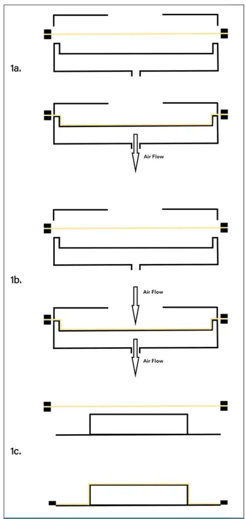
Vacuum forming is the process of heating a substrate to pliability and placing it around a mold. Air is vacuumed out, forcing the plastic around the mold to create the finished part (see Figure 1a).
Pressure forming is the same process as vacuum forming but is assisted by pressure from compressed air applied above the thermoplastic, forcing the material down (see Figure 1b).
Drape forming or drape molding is the process of heating the substrate to pliability and placing it over a mold and letting the material fall over the mold without the use of air or vacuum (see Figure 1c). Drape forming is economical, but it is a very slow process.
Going from 2D to 3D
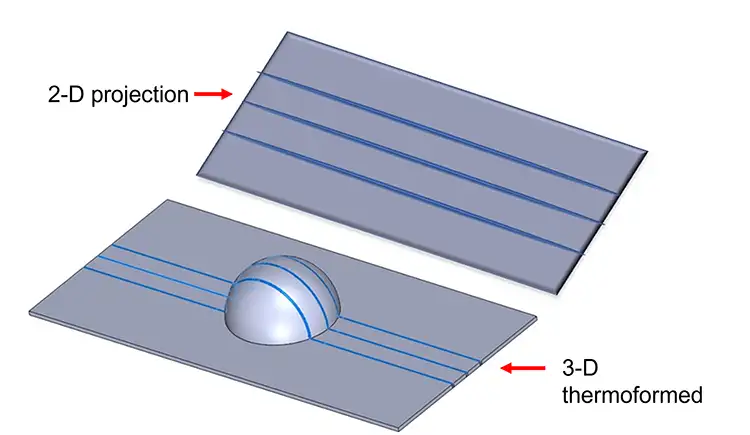
It should be noted here that if a pattern – for example, a pattern of conductive trace lines – is written on a 2D substrate prior to thermoforming, then post-thermoforming, the pattern will be translated into a 3D form (see Figure 2a). It should further be noted that pattern construction through thermoforming is a simple and fast process because its precursor step, i.e., printing on a 2D surface, is an already well-developed technology with many techniques in its gamut, e.g., slot-die, screenprinting, doctor-blading, gravure printing, etc. These printing techniques can produce conductive traces at various levels of resolution, currently in 10s of µms.
The initial printed pattern which occupied only the x-y plane now is pulled into the z-direction, not necessarily perpendicularly but in conformity to the surface of the mold. In the process, the total geometric area of the stretched surface increases, and it can be so only at the cost of width and thickness at the spots which have been pulled as domes. Further, depending on the initial trace line thicknesses, the lines may suffer deformation to the detriment of their functionalities. However, there has been R&D progress to mitigate this problem.
Naturally, the thermoforming process involves a complex deformation of the thermoplastic substrate when the 2D planar thermoplastic film converts itself to the 3D form. Therefore, the pattern written on a 2D surface may get distorted and non-uniformly stretched and strained. A good way of specialized printing on 2D to minimize distortion during molding is to undertake a simulation using the finite element method (FEM) by taking into consideration the thermomechanical properties of the substrate. FEM can create a pre-distorted 2D pattern onto which the conductive ink (or even dielectric ink) would be printed [2]. Such a systematic simulated approach faithfully will generate the desired pattern in 3D after the thermoforming. A simple schematic depicts this in Figure 2a. Currently, the most common substrates being used are polycarbonate, ABS, PMMA, styrene, polypropylene and PVC. They are suitable for the usual thermoforming temperature ranges, from 250° F to 425° F.
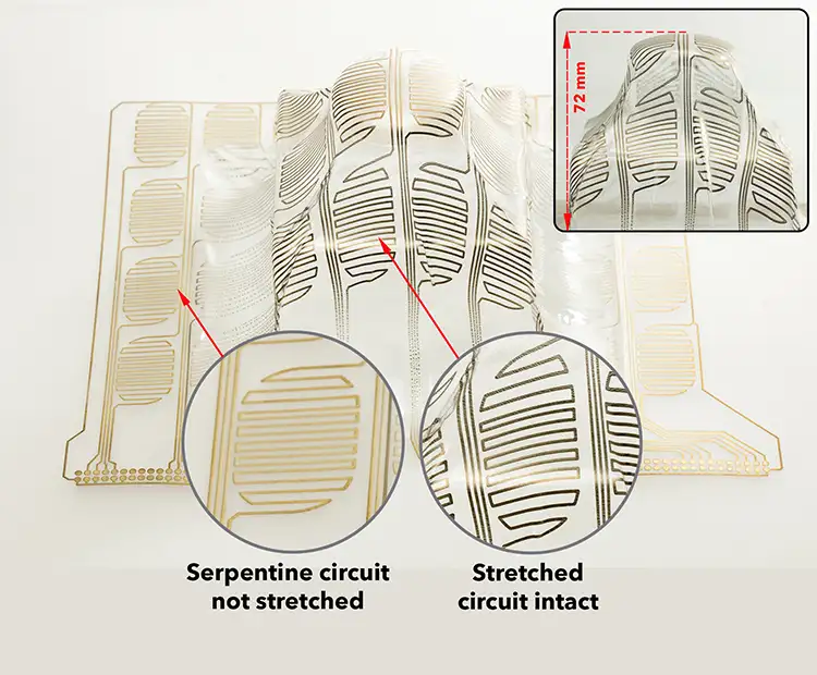
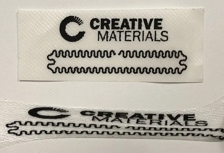
The inks to print should have good stretchability so that there is no macroscopic break and discontinuity of the electronic circuit. The currently used inks are eutectic gallium-indium–based liquid metal mixed with copper microparticles (EGaIn-CP) and some commercially available silver ink. Presently, this firm has been experimenting with creating circuits by using silver ink on a thermoformed polycarbonate surface and assessing circuit integrity (see Figure 2b).
Understanding silver-ink conductivity
The electrical conductivity of silver ink, which is composed mainly of silver flakes and polymer resins, can be understood by a percolation model of a conductor-insulator composite [3]. The conductivity of the composite can be expressed as
σc =σf(f-f*)t
where
σc = conductivity of the composite,
σf = conductivity of the filler, i.e., the silver,
f = filler fraction, i.e., the silver fraction,
f* = critical filler fraction, meaning at the percolation threshold, and
t = a conductivity exponent
It is apparent from the above equation that if the filler fraction reaches the critical limit, the factor (f-f*)t will change rapidly due to the exponential dependence. Hence, in a thermoformed 3D scenario, if the printed ink undergoes a large strain, depending on the initial silver fraction in the ink, there may be circumstances where the critical limit is reached at certain spots. This can raise the resistance of the circuit severely and compromise its integrity.
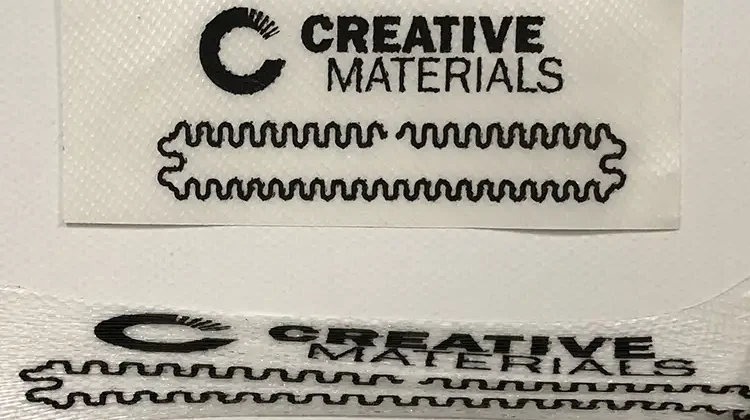
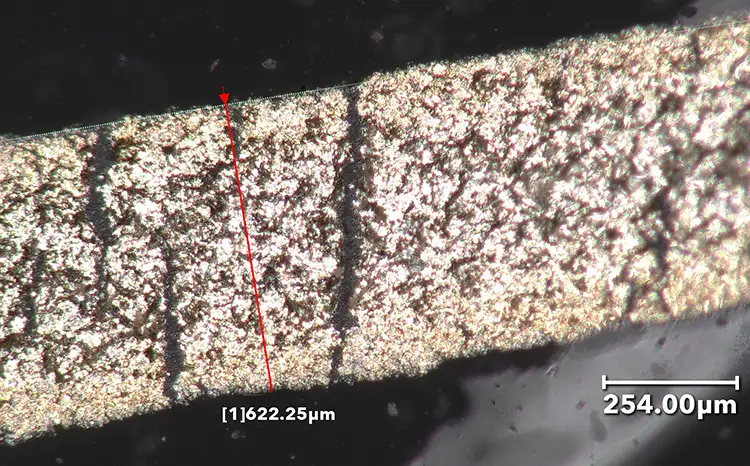
The development of cracks on the silver trace line may be noted in Figure 3. A way to reduce the probability of cracking is in preferring meandering patterns so that the strain is not causing a unilateral distancing of the conducting domains, but rather is assisting in evenly compressing the distances between them at the angular regions (see Figure 4) [4]. This effect has been encountered in this firm’s experiments with silver ink on a polycarbonate surface (see Figure 3) and has required several iterations.
Conclusion
In summary, thermoforming is a simple design tool for printed electronics. By making patterns on a planar 2D surface by any chosen print method, designers can embed the patterns onto a 3D object while bypassing the complex tooling needed to navigate surfaces of arbitrary curvatures. Thermoforming comes as a handy tool for constructing conformal interconnects economically.
References
- “Thermoforming,” https://www.nazdar.com/en-us/News-events/ArtMID/4165/ArticleID/291
- Customizable, conformal, and stretchable 3D electronics via predistorted pattern generation and thermoforming, Choi et al., Sci. Adv. 2021; 7: eabj0694.
- Cohen, M.H., Jortner, J., Webman, I., 1978. The electronic properties of inhomogeneous materials; metal–nonmetal transitions. In: Garland, J.C., Tanner, D.B. Eds., Electrical trans- Ž .port and optical properties of inhomogeneous Media, AIP Conf. Proc. No. 40, American Institute of Physics, New York, p. 63.
- “Analysis of electrically conductive silver ink on stretchable substrates under tensile load,” Merilampi et al., Microelectronics Reliability, 50 (2010) 2001–2011.

Yudhisthira Sahoo, Ph.D., technology specialist, is FLEXcon’s technical lead on the scouting and feasibility of new technology within the Business Technology & Discovery group. He has an interdisciplinary education background with a Master’s in Chemistry and Ph.D. in Physical Sciences. Including College and University teachings, Yudi has 28 years of R&D experience in materials-science research on various topics, such as electronic transport in glassy solids; nanomaterials syntheses; thin-film devices, such as photoconductors, photovoltaics, batteries and printed heaters; and more.

Christopher Kowalczyk is FLEXcon’s Incubator Team Lead in the Business & Technology Discovery group working to increase manufacturing readiness of new technologies by identifying how roll-to-roll operations can be leveraged in the manufacture of new products. This includes rapid prototyping, identifying new equipment and creating new processes with a goal of determining the viability of opportunities and projects in their infancy. Chris has a history of over 22 years in polymeric coating and laminating encompassing production, lean methodology and innovations in R2R capabilities.

Mike Merwin, manager-Business & Technology Discovery group at FLEXcon Company, Inc. (Spencer, MA), has worked with polymeric coating for over 40 years and has served in a variety of roles in technical service and product development creating functional technologies for existing and emerging markets. He is a member of the Society of Plastic Engineers and the US Dept. of Energy/Advanced Manufacturing Office, serving on the Industry Engagement Panel for R2R Collaboration.
More info: 508-885-8200, fax: 508-885-8400, www.flexcon.com

