
By Seunghoon Lee, Ph.D., senior researcher, Korea Institute of Materials Science (KIMS)
Editor’s Note: This technical paper is based on a presentation at the 2019 AIMCAL R2R Conference Asia, held in Daejeon, South Korea, in May 2019.
Abstract
We introduced ion-beam web treatments for the fabrication of polymer films with a nanostructured surface. A linear ion-beam source generated energetic, gas-ion beams with an energy of up to 3 keV. The ion-beam irradiations on polymer substrates resulted in ion-induced surface instability, which caused sputtering, cross-linking and heating. The surface reactions in turn resulted in self-organization in the form of wrinkles, dimples and ripples in the nanostructures. The ion-beam irradiated films with fabricated nanostructures are used as anti-reflective films and water-repellent films.
Introduction
Polymer films with surface structures ranging from tens to hundreds of nanometers have been used in various fields due to their unusual optical and mechanical properties. The nanostructured surface with hydrophobic coating can be attached to buildings, automobiles, solar cells, etc. A polymer film with a wavelength of tens to hundreds of nanometers smaller than visible-light wavelength can be applied as an antireflective film for both indoor and outdoor displays. Recently, nanostructured surfaces have been studied using surface-enhanced Raman spectroscopy, which uses localized, surface-plasmon resonance for biosensing [1].
There are various methods for producing a nanostructured surface (nanosurface) of polymer films, such as lithography-reactive ion etching (RIE), imprinting, plasma treatment and heat treatment. Lithography-RIE and imprinting methods using patterning techniques produce nanosurfaces with good regularity. Nanosurfaces with good regularity show excellent optical properties, but their application requires high manufacturing cost. On the other hand, irregular nanosurfaces prepared by plasma treatment or heat treatment do not show excellent optical properties, but can be used in antireflective, water-repellent and localized surface-plasmon resonance applications due to relatively low manufacturing cost. Therefore, it is important to properly select a manufacturing technique in terms of productivity and cost ratio depending on the use of the nanosurface polymer film.
Vacuum plasma R2R surface treatment
Korea Institute of Materials Science (KIMS) is studying vacuum plasma roll-to-roll (R2R) surface treatment technology for polymer films. This study involves the use of ion-beam sources for the fabrication of polymer films with nanostructure surfaces and for controlling interfacial properties between the deposited layer and the films. Closed-drift-type ion sources are used in the R2R surface treatment. Sub-meter ion sources and R2R surface treatment technologies are available for various film sizes [2]. Researchers at KIMS have focused on studying the improvement of the adhesion of CIGS thin films, the adhesion of flexible copper-clad laminate (FCCL) seed layer, the manufacture of an antireflective nanostructured film and the manufacture of an antireflective and super-water-repellent functional window film using ion sources and physical vapor deposition (PVD). Recently, research has been focused on identifying the mechanism of nanostructure formation formed by ion-beam irradiation on the surface of polymer films.
The mechanism of nanostructure formation by ion-beam irradiation is related to the collision reaction between the polymer medium and the ions (see Figure 1). Gas-ion particles (with energies of hundreds to thousands of eV) collide on the surface of the polymer film fabricated via the R2R process. Ions collide with the constituent elements of the polymer and transfer their kinetic energy to the film. Depending on the amount of energy transferred by ions and the collision targets (nuclei and electron), the polymer components respond by undergoing ionization, displacement and vibration. Compared with that of metals and semiconductors, polymers have a lower density, resulting in low energy absorption per unit transmission distance of ions; energy absorption of metals and semiconductors is 30–50 eV/Å, while that of polymers is 15–30 eV/Å. Therefore, when ion beams are irradiated on the polymer surface, displacement and vibration reactions occur rather than ionization (see Figure 2).
![FIGURE 2. Linear energy transfer of impinging ions on polymer surface, numerical calculation result from SRIM [3].](https://convertingquarterly.com/wp-content/uploads/2025/02/cq320lee_fig2.jpg)
Phenomena caused by ion-beam irradiation
Displacement of polymer surface elements by ion-beam irradiation causes phenomena such as scission, cross-linking, vacancy generation and sputtering on the surface. The polymer component produced by scission due to ion collision is called recoil, and the recoil moves through the medium and collides with other polymer components to produce another recoil. Recoils move and settle in unstable locations, causing cross-linking. On the other hand, recoil that moves to the surface of the film causes sputtering by leaving the surface if it has more energy than does the surface binding energy. If the energy of the recoil is insufficient to cause additional displacement, the energy is dissipated as heat by phonon vibrations. The heat release acts as a cause of cross-linking of the polymer film.
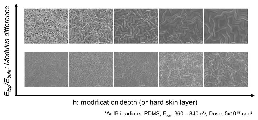
The ratio of sputtering and cross-linking of the polymer film surface caused by ion-beam irradiation determines the shape of the nanostructure formed. Cross-linking mainly is observed when gas-ion beams of 2 keV or less are irradiated on low-density PDMS and PU. The polymers such as PDMS or PU have a density of 0.8 g/cm3. Therefore, the energy delivered to the recoil is not sufficient to induce scission, so generally, cross-linking occurs. However, when ions collide with the top layer of the polymer, some sputtered surface is observed, but it alone does not control the overall structure of the nanosurface. The polymer surface where cross-linking mainly occurs is wrinkled due to the difference in elastic modulus with that of the base material, and the formula well explains the width or the period of the wrinkle due to the mechanical properties of the cross-linked surface (see Figure 3). The most representative example is the case where the oxygen ion beam is irradiated on the PDMS surface. When the oxygen ion beam is irradiated on the PDMS surface, the surface of SiO2 bond increases, causing a large elastic modulus difference between those of the surface and the base material.
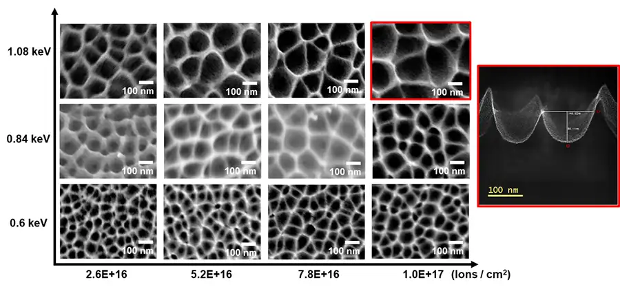
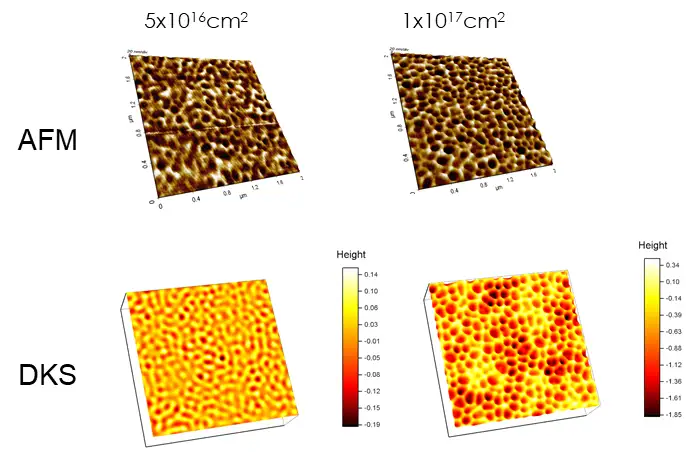
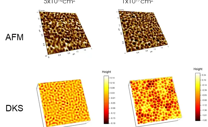
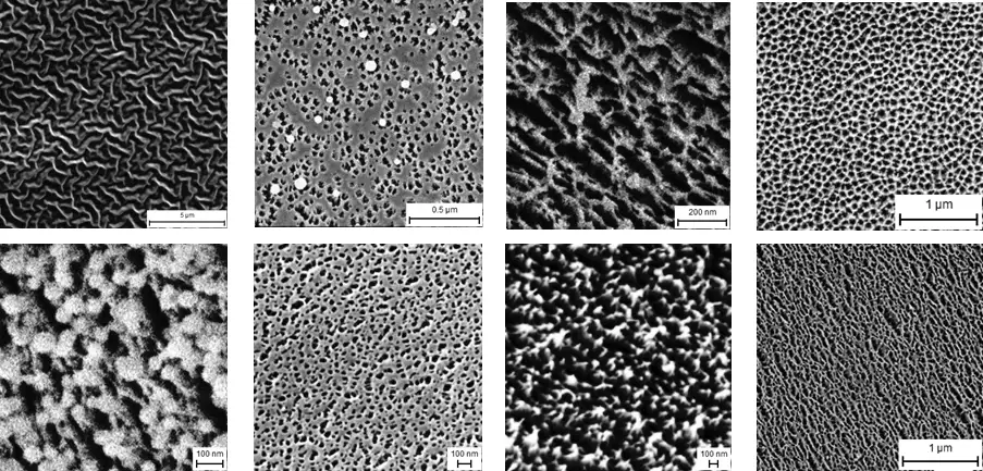
When sputtering is mainly caused by cross-linking due to ion-beam irradiation, surfaces with dots, dimples, ripples, etc. are formed (see Figures 4-5). Polymers that are mainly sputtered by ion-beam irradiation are materials with a density of 1.3 g/cm3 or more, such as PET, PEN, PI and PTFE. Nanostructure formation by sputtering can be classified into two types. Firstly, when semi-crystallization of the polymer surface occurs by ion-beam irradiation, the sputtering yield difference between crystalline and amorphous phases results in nanosurfaces. It has been reported that cross-linking by ion-beam irradiation causes semi-crystallization, which allows worm-like surfaces to be obtained on PTFE films. Secondly, in the absence of semi-crystallization, nanostructures are formed by instability caused by ion collisions on the polymer surface. Surface instability induced by ion bombardment has been widely studied in metal and semiconductor materials. When the ions collide with the surface, the sputtering rate difference depending on the curvature of the surface is generated, and the surface structure is formed as the amount of ion dose increases.
After Bradley-Harper proposed the theoretical model to describe this morphology formation, various continuum equations were proposed by various researchers to explain the actual phenomena and were verified by various experiments [4]. Several continuum equations, such as the damped Kuramoto-Sivashinsky model and general continuum model, have been proposed [5]. Continuous equations have been studied only on metal and semiconductor surfaces, but recently we have tried to explain the nanostructures produced by ion-beam irradiation through continuous equations by applying them to polymer surfaces where sputtering occurs.
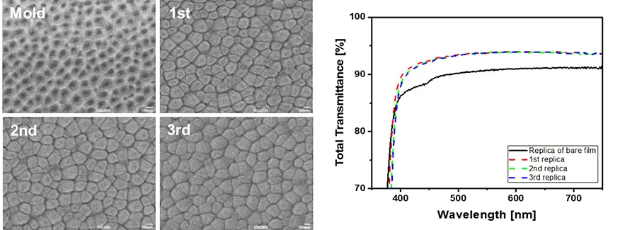
Polymer films with a nanostructured surface have been applied to fabricate anti-reflective polymer films using a soft molding method (see Figure 6). On polymer surfaces, we fabricated nanostructures, which have an opposite shape of moth-eye. The polymer films were used as a soft mold to squeeze a moth-eye structure on UV-curable resins. Anti-reflective structures were transferred successfully to the curable resin. The anti-reflective films showed transmittance values of up to 93%.
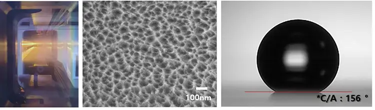
Ion-beam irradiation on PET films has been applied to hydrophobic film fabrications (see Figure 7). Gas ion-beam irradiation induced sharp nanosurfaces, which are useful to make a water-repellent surface. After the ion-beam treatment, a fluorine-based self-assembled monolayer was coated on the nanosurface. The water contact angle was up to 156°. The production speed was 0.20 mpm with a linear ion-beam source.
Conclusion
Ion-beam irradiation of polymer substrates made it possible to fabricate the nanosurface films with a simple R2R process. The structure of nanosurface is controllable using the continuum equation. The self-organization nature of ion-beam irradiated polymer surfaces could expand the applications of nanosurface polymer films.
References
1. S. Park, X. Xiao, J. Min, C. Mun, H.S. Jung, V. Giannini, R. Weissleder, S.A. Maier, H. Im, and D. Kim, Advanced Functional Materials. 29, 1970296 (2019).
2. S. Lee, E.Y. Byun, J.K. Kim, and D.G. Kim, Current Applied Physics. 14, S180 (2014).
3. J.F. Ziegler, M.D. Ziegler, and J.P. Biersak, Nucl. Instruments Methods Phys. Res. Sect. B Beam Interact. With Mater. Atoms. 268, 1818 (2010).
4. R.M. Bradley and J.M.E. Harper. Journal of Vacuum Sciences & Technology. A Vacuum, Surfaces, Film. 6, 2390 (1988).
5. A. Keller and S. Facsko. Materials (Basel). 3, 4811 (2010).
Seunghoon Lee, senior researcher with the Korea Institute of Materials Science (KIMS) in Changwon, South Korea, holds a Bachelor of Science and a Master of Science in Nuclear Engineering from Seoul National University. He received his Ph.D. in Physics from Korea Advanced Institute of Science and Technology (Daejeon, South Korea). Since 2008, Lee has been with KIMS, where his current research is focused on the fabrication of nanomaterials by ion-induced surface instability and atmospheric-pressure plasma for bio-surface treatment. He can be reached at +82-55-280-3512, fax: +82-55-280-3570, email: seunghun@kims.re.kr.