

By Dr. Khasha Ghaffarzadeh, CEO, TechBlick
Printed electronics are everywhere and can be found in applications as diverse as a smart diaper to a precision missile. This article will highlight some application and technology development examples for roll-to-roll (R2R) printed electronics and the end-use markets they serve, including healthcare, packaging, photovoltaics, displays and beyond. The common thread here is R2R printing of electronics, regardless of printing technique, e.g., screen, flexo, gravure, slot-die, etc. The applications reviewed herein are presented randomly and follow no particular order of importance. The images and examples below are extracted from 2021 presentations offered by this firm, which is a global information resource for printed, flexible, hybrid and in-mold electronics.
Editor’s Note: Part 1 of this article covered medical sensors, photovoltaics, smart pharmaceutical packaging and displays in the 2021 Q4 issue, pages 29-31.
Displays

Printed-electronics displays have advanced tremendously over the past 10-15 years. From yesterday’s black-and-white e-readers such as the Kindle® to today’s full-color, high-resolution foldable smartphones, displays are everywhere in a wide variety of applications (see Figure 4).
R2R printing is and can be used in other types of more complex displays. In quantum dot (QD)-LCD displays, the enhancement QD film is R2R slot-die-coated (see Figure 5 far-right image). This is a commercial success story.
Printing also may play a role in the emerging microLED technology. It can be used to print wraparound interconnects connecting the front side and backside of the glass substrate. It also can deposit bumps, connection pads, etc.
Early-stage development work is underway to explore the possibility of some type of R2R process for placing the microLEDs themselves. Here, I highlight one early-stage approach based on the LIFT (laser-induced, forward-transfer) process, followed by R2R rapid photosintering on low-temperature substrates using standard solder.
In LIFT, a laser pulse is shone through a patterned transparent carrier. The laser hits a proprietary release coating, which releases the material or the component. The roadmap shown in Figure 5 on the left is by Holst Centre, showing how it first demonstrated, on a small-scale machine, narrow-line deposition of materials before progressing the technology toward component transfer. Recently, Holste demonstrated the use of LIFT to transfer 40x40x50-µm3 microLEDs with 80-µm gap and 500-µm interconnects. This lab-scale demo had a (relatively) low yield of 98%, with 20% of LEDs ending up on their side. These results are far from production-ready, but they establish a roadmap with large improvement potential. This technique, when combined with R2R photosintering, offers the chance to develop a fully R2R process.

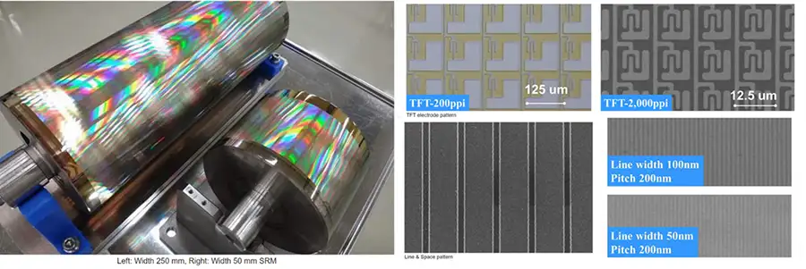
Fine-line R2R printing
There is tremendous progress in fine-line R2R printing. Figure 6 shows examples of work from Asahi Kasei in Japan. The company has developed a seamless roller mold (SRM) using electron-beam lithography to achieve high-resolution, seamless R2R-imprinted films. Some results also are shown below, demonstrating the ultrafine feature capability of this R2R process. The application is close to commercialization, especially as a transparent RFID for track-and-trace applications.
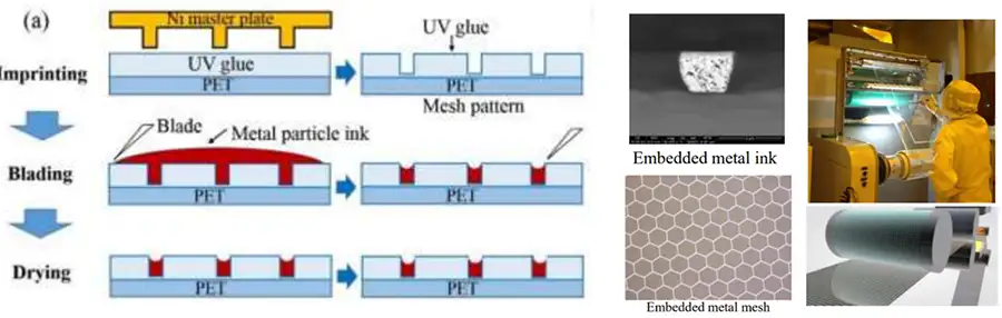
R2R nanoimprinting can create ultrafine features. Figure 7 shows a hybrid-R2R continuous process, developed by Printable Electronics Research Centre in Suzhou, China. The process enables the formation of ultrafine features (<5 µm), such as embedded metal-mesh structures aimed at transparent touch and heating applications. The left schematic in Figure 7 shows the process flow. Note that the embossing takes place using a rolling nano-embossing drum. The center images show the metal-mesh pattern and the embedded nature of the conductive lines, which enable one to thicken the line to achieve higher conductivity without compromising surface smoothness. The right image shows a web-processing machine previously deployed by O-Film to commercially R2R-produce these metal-mesh touchscreens. At its peak, 1.5 million such panels were produced annually.
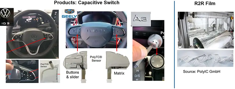
Automotive
A major trend in the automotive industry is the replacement of mechanical switches with capacitive ones. Figure 8 from PolyIC GmbH (a Kurz Co.) shows an R2R-printed, transparent touch film integrated inside the driving wheel or gear of a vehicle. The transparent sensors are a R2R-printed metal-mesh film, consisting of 100-nm-thick silver nanoparticle inks printed with a linewidth and spacing of 10 µm and 100 µm, respectively. The exact R2R printing technique is proprietary.
R2R hybrid-RFID printing
As a final topic to close our review, I would like to mention R2R RFID printing and how it is evolving toward R2R production of complex multi-chip hybrid circuits. An example is Smooth & Sharp (S&S) in Taiwan, which initially developed R2R manufacturing of near-field communication devices (NFC) on paper. These NFCs were at least 2x the price of the company’s conventionally manufactured on-plastic counterparts two years ago. Now, S&S indicates that price-parity has been reached, which can help render more end-use markets accessible.
Importantly, this also was the start of the technical development where the NFC antennae have one small chip and a single metallization layer. In the future, R&D will work toward more chips, more layers and more complicated circuit designs. Projects include the integration of a two-chip (NFC and LED) tag, development of an 11-component piece (two active layers and 10 passive components), and the demonstration of a six-layer tag that is R2R-printed on paper.
This is a very promising trend overall. Manufacturing for flexible hybrid electronics (FHE) still is in its relatively early stages of development but is advancing. New ultrathin flexible chips, either natively flexible or thinned down, are becoming available. Currently, with the help of RDLs (re-distribution layers), these packages become capable with the resolution of printed lines on flexible substrates. In addition, low-temperature attach techniques (photosintered solder, ultra low-temperature solder or particle-aligned conductive adhesives) are emerging to enable component attachment to PET films and specialty papers. This is the initial roadmap toward R2R manufacturing of complex hybrid electronics.
Conclusion
In summary, we demonstrate that R2R-printed electronics really are everywhere with numerous and growing end-use applications across many markets. It is a vibrant and fast-evolving landscape of new technology, ecosystems, and material & production processes.
Khasha Ghaffarzadeh, CEO of TechBlick (Frankfurt, Germany), holds a Master’s degree and Ph.D. from the University of Cambridge and University College London, respectively. During his Ph.D., he worked with Samsung (SAIT) to produce and characterize state-of-the-art, amorphous metal-oxide TFTs. Khasha spent more than a decade leading a global analysts team focused on emerging technologies at IDTechEx. Khasha and his team scout the technology landscape and the global ecosystem to curate presentation agendas. He is a regular presenter at conferences in his areas of expertise, delivering keynotes as well as masterclasses. His work was published in leading academic journals such as Nature, receiving more than 1,000 citations. Khasha can be reached at +49-17-661-70413, email: khasha@techblick.com, www.techblick.com.