By Matthew Dyson, Ph.D., senior technology analyst, IDTechEx
Printing electronics as easily as newsprint has long been a compelling vision, promising cheaper circuits, sensors, solar panels and even displays. Known as roll-to-roll (R2R) electronics, it uses conductive and other functional inks printed onto flexible substrates. However, for many applications, R2R electronics has been held back by difficulty incorporating processing capabilities and a lack of high-volume applications. Flexible hybrid electronics (FHE) that employ mounted components largely resolve this technical issue, while there is a rapidly growing demand for low-cost sensors for applications such as electronic skin patches. With increasing investment from larger players, it seems that R2R electronics might finally be here.
Introduction
Appreciating the potentially transformative nature of roll-to-roll (R2R) printed electronics requires an understanding of what it replaces. At present, most electronic circuits are rigid, printed circuit boards (PCBs), which somewhat confusingly are not actually printed. Instead, boards of FR4 are laminated with a thin layer of copper, which then is selectively etched to leave the desired wiring pattern on a green-colored substrate. A similar process produces conventional flexible, printed circuit boards (FPCBs), except that the rigid FR4 is replaced with flexible orange polyimide.
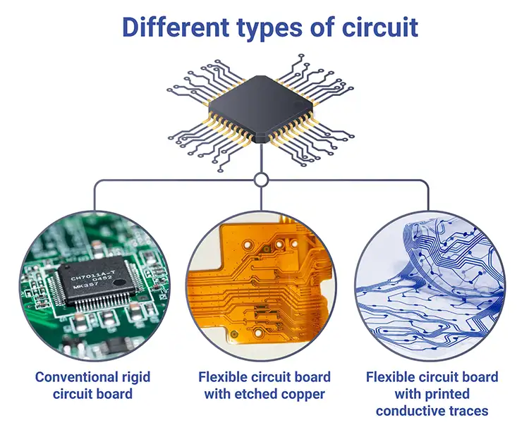
In contrast, printed electronics is an additive rather than subtractive technique (see Figure 1). The conductive traces (i.e., wiring) simply are printed from conductive ink onto a substrate, which can be flat or curved, rigid or flexible. Additive manufacturing brings a sustainability and bill-of-materials benefit because less conductive material is used and none is wasted – although, as the wiring is made from conductive ink rather than pure metal, conductivity generally is reduced. Furthermore, if the printing method is digital, such as inkjet, then no masks or clichés need to be made and each circuit can have a different design.
Whether printing or etching, using flexible substrates enables the option of R2R manufacturing. Rather than handling discrete collections of circuits via sheet-to-sheet (S2S) manufacturing, the continuous process enables circuitry to be produced at much higher throughputs and hence lower unit costs. R2R production already is standard practice for RFID-tag manufacturing, with billions of tags produced each year.
Overcoming adoption barriers
The high throughputs and lower costs make R2R-electronics manufacturing highly compelling and a great opportunity for the converting industry. However, outside of RFID and a few niche applications such as LED strip lights, R2R-electronics manufacturing is not yet widely adopted.
Gaining greater adoption requires overcoming three main challenges: component attachment, quality control and finding a large enough market. Of course, these challenges need to be met while simultaneously improving the sustainability of the manufacturing process.
Component attachment
Regardless of whether the conductive traces are printed or etched, mounting electrical components such as resistors, capacitors and integrated circuits (ICs) to continuous flexible substrates to form a hybrid circuit can be challenging. Industry standard pick-and-place machines generally are used, but these require the substrate to be stationary while the components are placed. As such, for all but the simplest circuits, this component placement time generally is the rate-determining step. Furthermore, if the substrate is stretchable, such as for wearable electronics, then aligning the components correctly is difficult as simply having optical-registration patterns in the corners of the circuit is insufficient.
Ensuring durability is another challenge when attaching rigid components to flexible or even stretchable substrates. This is due primarily to the discrepancy in thermal expansion coefficients, which can lead to solder or electrically conductive adhesive (ECA) fracturing when the hybrid circuit undergoes thermal cycling. The contrasting mechanical properties between substrate and component also can lead to detachment if the substrate repeatedly is flexed or stretched. Various solutions have been proposed, including using stretchable ECAs or having “rigid islands” where there is less stretching or flexing.
Quality control
Another technical requirement to commercializing R2R-electronics manufacturing, especially if printing rather than etching, is ensuring reproducibility. In conventional S2S circuit manufacturing, the viability of the final circuit with attached components typically is checked using flying probes to make electrical contacts. These still can be employed with R2R manufacturing but need a stationary substrate; this either slows down the process or requires coordination with paused substrate movement for component attachment.
When printing conductive traces, conductivity can be highly dependent on processing conditions. Even seemingly inconsequential factors such as nozzle temperature or how long the ink has been sitting prior to printing can affect both the conductivity and the print resolution. This processing-condition dependence creates a substantial entry barrier to companies aspiring to have a novel, and often higher conductivity, ink introduced into an existing printing system because extensive (and expensive) process engineering may be required.
High-throughput R2R manufacturing magnifies these concerns since, if the properties of the printed ink deviate from acceptable tolerances when the finished circuit is assessed, large amounts of expensive material can be squandered. The solution is in-line monitoring, which is receiving increasing emphasis for suppliers of R2R printed-electronics production lines. The most common approach is high-speed cameras coupled with image analysis algorithms to determine print resolution, line continuity and unwanted droplet splatter. In-line conductivity monitoring also presents an innovation opportunity with novel methods, such as terahertz spectroscopy, being used to monitor conductivity in real-time.
Finding a suitable market
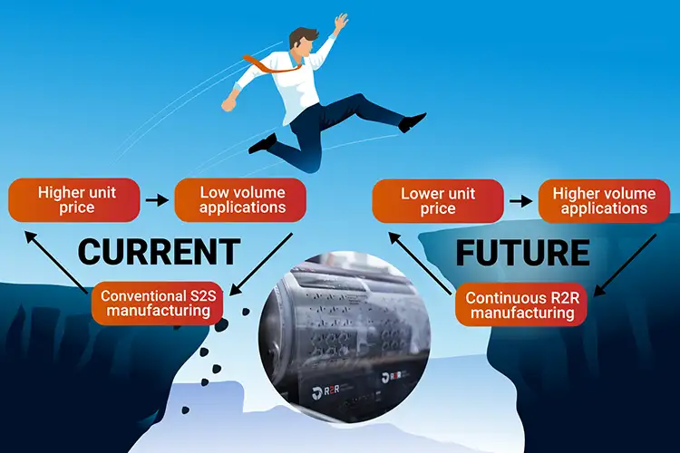
The main commercial challenge for R2R-electronics manufacturing is finding a market that requires extremely high volumes of identical circuits. While if run at capacity, the high throughput means that the cost of manufacturing equipment per circuit produced is extremely low; this is, of course, reliant on using that capacity (see Figure 2).
Two emerging applications that will require very high volumes of identical, simple, low-cost circuits are smart packaging and electronic skin patches because both will be at least partially disposable. However, to date, neither of these applications has been significantly realized; they only are economically viable for most use cases if the unit cost is very low. Despite the great potential to add value – for example, by reducing food waste and enabling continuous health monitoring – these technologies are to some extent constrained by the following cycle: the unit cost isn’t low enough for high-volume applications, so R2R manufacturing isn’t applicable, and so the unit cost isn’t low enough.
Enabling high-mix, low-volume (HMLV) R2R-electronics manufacturing is a promising strategy to resolve this cost-volume conundrum and target a wider range of applications. This would require transitioning from analog to digital printing methods, such as from screenprinting or flexography to inkjet. With digital manufacturing, much smaller batches of circuits can be produced, even on the same roll of substrate, without additional costs per unit.
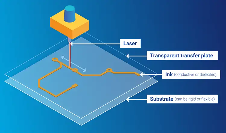
At present, inkjet printing is by far the most common digital-printing method. While widely used for graphical ink, both domestically and commercially, the nozzles associated with inkjet printing can cause difficulties when printing conductive inks. An emerging, alternative digital-printing method that aims to resolve these issues is laser-induced, forward transfer (LIFT). Rather than using nozzles, the ink is coated onto a flat glass “transfer plate” and selectively transferred to the underlying substrate using a laser that heats the solvent and causes an ink droplet to be ejected from the transfer plate (see Figure 3). A wide variety of ink viscosities can be used because there is no risk of nozzle clogging, and deposition is extremely fast as there are no mechanical moving parts. Integrating LIFT technology into a R2R-production line for printed electronics would enable high-throughput digital manufacturing with fewer material constraints and process engineering requirements than inkjet.
Sustainability
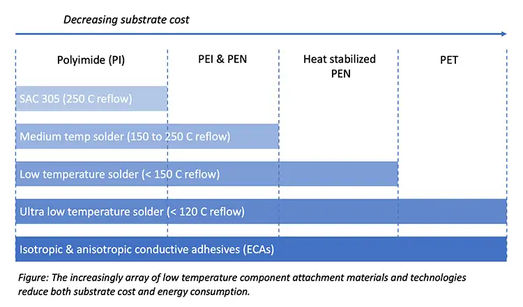
Improving the sustainability of electronics manufacturing is a major focus of many manufacturers, partly motivated by pressure from end users to reduce “Scope 3” emissions (i.e., those produced in the supply chain). Because a large proportion of the energy in electronics manufacturing comes from heating the ovens used for solder reflow, reducing processing temperatures is essential. Competing approaches, all of which maintain the self-alignment benefits of solder relative to electrically conductive adhesives (ECAs), include bismuth-containing solders with a much lower reflow temperature and photonic soldering using rapidly pulsed, bright white light. Reducing the temperature required for component attachment also enables much cheaper but thermally fragile substrate materials, such as PET, to be used (see Figure 4).
The higher throughput of R2R-electronics manufacturing relative to conventional S2S approaches also brings extrinsic sustainability benefits. Because throughput is much higher, the factory footprint can be much smaller to produce the same number of circuits. Additionally, reduced labor costs associated with high-volume continuous production, especially with largely automated in-line process control, means that manufacturing can be located much closer to the final market. This obviously cuts shipping distances and improves supply-chain security, especially as most circuits currently are manufactured in Asia.
Conclusion
Overall, there is huge potential for R2R manufacturing to produce printed and flexible electronics, especially for emerging high-volume applications, such as smart packaging and electronic skin patches. Digital manufacturing, which facilitates the decoupling of volume and unit cost, could enable R2R-electronics applications to grow much wider.

Matthew Dyson, senior technology analyst at IDTechEx, holds a Bachelor of Science Joint Honours (first class) degree in Physics and Chemistry from Durham University (UK), and an MRes (with distinction) and Ph.D. in Physics from Imperial College London (UK), focusing on organic electronics. His academic research, which has been cited over 500 times, also included work on perovskite and organic photovoltaics. This was followed by two years as a post-doctoral researcher at Eindhoven Technical University (Netherlands), focusing primarily on organic photodetectors (OPDs). At IDTechEx, Matthew analyses technical innovations and market opportunities across the printed and flexible electronics landscape and manages a team of technology analysts covering wearable technology, AR/VR and emerging photovoltaics. He can be reached at +44-1223-827-631, email: m.dyson@idtechex.com or www.IDTechEx.com.

