By Mike Simmons, president & CEO; Matthew Kleyn, Joseph Vlach, and Liz Josephson, Intellivation LLC
Laser patterning of conductive, vacuum-deposited thin films for production of low-cost / high-throughput, flexible-electronic devices provides versatility, accelerated development cycles and manufacturing scalability. Optimizing performance by adjusting device architecture or geometry can be done in real-time by altering laser-scanning patterns without impacting cost of materials, time, or additional resources, e.g. mask fabrication. Surface roughness directly impacts the success of laser patterning; surface morphology affects the continuity and adhesion of successive sputtered thin-film layers and their final performance. Laser patterning can be used to tune the surface roughness to control the flow of fluids. Low-cost, high-volume production of sensors can be achieved through the integration of laser technology in a roll-to-roll (R2R) system with in-situ quality control.
Editor’s Note: This technical paper is based on the company’s presentation at SEMICON® WEST / FLEX 2023 held in San Francisco, CA, in July 2023.
In the fast-evolving landscape of electronics, the demand for high-performance devices with enhanced functionalities, such as mechanical flexibility, continues to grow. One notable technology that has garnered significant attention is the use of 2D devices. These materials, such as graphene and MoS2, exhibit unique electrical and mechanical properties that make them ideal for flexible-electronics applications and enable high-rate roll-to-roll (R2R) fabrication. To meet the rising demand and requirements for flexible, 2D-microelectronics devices, we are exploring innovative manufacturing techniques, including the use of vacuum coatings in combination with laser technology. Laser patterning of sputtered coatings has emerged as a promising method for achieving high-volume production with precision, functionality and efficiency for a wide range of flexible applications.
Sputtered coatings as a foundation
Sputter deposition is a widely used technique for depositing thin films onto substrates. In the context of flexible, 2D microelectronics, sputtered coatings serve as the foundation for building functional devices. Sputtering involves bombarding a target material with ions to eject atoms or molecules, which then deposit onto a substrate to form a thin film. This process allows for precise control over the thickness and composition of the deposited film, making it a preferred method for creating uniform and reproducible coatings. Sputtered layers were deposited using this firm’s R2R Lab system.
Laser patterning for precision and scalability
While sputtering provides an excellent method for depositing coatings uniformly over large areas, laser patterning adds the ability to create discrete devices, circuits and other types of discontinuous features in the manufacturing process. Using these two techniques in combination provides unusual capabilities, particularly during product development. Traditional methods of patterning, such as photolithography, involve multiple steps and can be time-consuming. Traditional thin-film patterning methods require masks, templates and other components that require geometric commitment at an early stage of design, this can result in drastically slower development and is impacted by any change during the development. Masks also limit features to larger sizes and result in variation of feature dimensions and edge quality over the life of the mask. Laser patterning, on the other hand, offers a direct and efficient way to create and define patterns on sputtered coatings, including changes in geometry by redefining the path of the laser, while providing consistent feature size and edge quality.
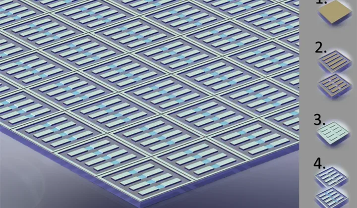
Laser patterning involves using a laser beam to selectively remove or modify specific areas of the deposited film. This process generates intricate patterns with submicron-level precision. Control and precision of the laser is critical for creating and modifying each layer for the specific end-use requirements. The non-contact nature of laser patterning reduces the risk of contamination and damage to the underlying substrate, making it particularly suitable for delicate 2D materials. This technique provides the ability to develop and then validate a design and process in small volumes and then easily transfer to large-area R2R production without changes to the laser-processing equipment (see Figure 1).
Advantages of laser patterning in 2D flexible-microelectronics manufacturing
- High precision:Laser patterning enables the creation of intricate features with submicron precision, ensuring that active regions in the device are precisely defined. This level of precision is crucial for optimizing device performance and achieving consistent results across high-volume production.
- Scalability: Traditional patterning methods may struggle to meet the demands of high-volume production due to their sequential and time-consuming nature. Laser patterning, being a rapid and non-contact process, is inherently scalable. It allows for the efficient production of large batches of devices without compromising on quality or performance.
- Flexibility in design: Laser patterning provides designers with greater flexibility in designing device architectures. This flexibility is particularly valuable as flexible-microelectronics technology evolves and new applications emerge. Engineers easily can adapt and optimize device architectures to meet the specific requirements of different industries and end-use cases.
- Reduced waste: The precision of laser patterning minimizes material waste by selectively removing only the necessary portions of the coating. This not only contributes to cost savings but also aligns with sustainable-manufacturing practices. Material compatibility allows for equipment versatility, changing materials of the stack and adapting laser settings to achieve desired results. This can be done simply and quickly and can include changes to the substrate. Reusability and versatility of equipment is not possible in many current 2D-manufacturing processes without a large effort to retrofit or change equipment for each process step change.
- Speed and efficiency: Laser patterning is a fast and efficient process, allowing for rapid prototyping and quick iterations in the design and manufacturing phases. Equipment versatility with high-speed lasers allows for faster processing including the ability to add more lasers to increase production ramping without the addition of large investments. This speed is essential for staying competitive in the fast-paced electronics industry.
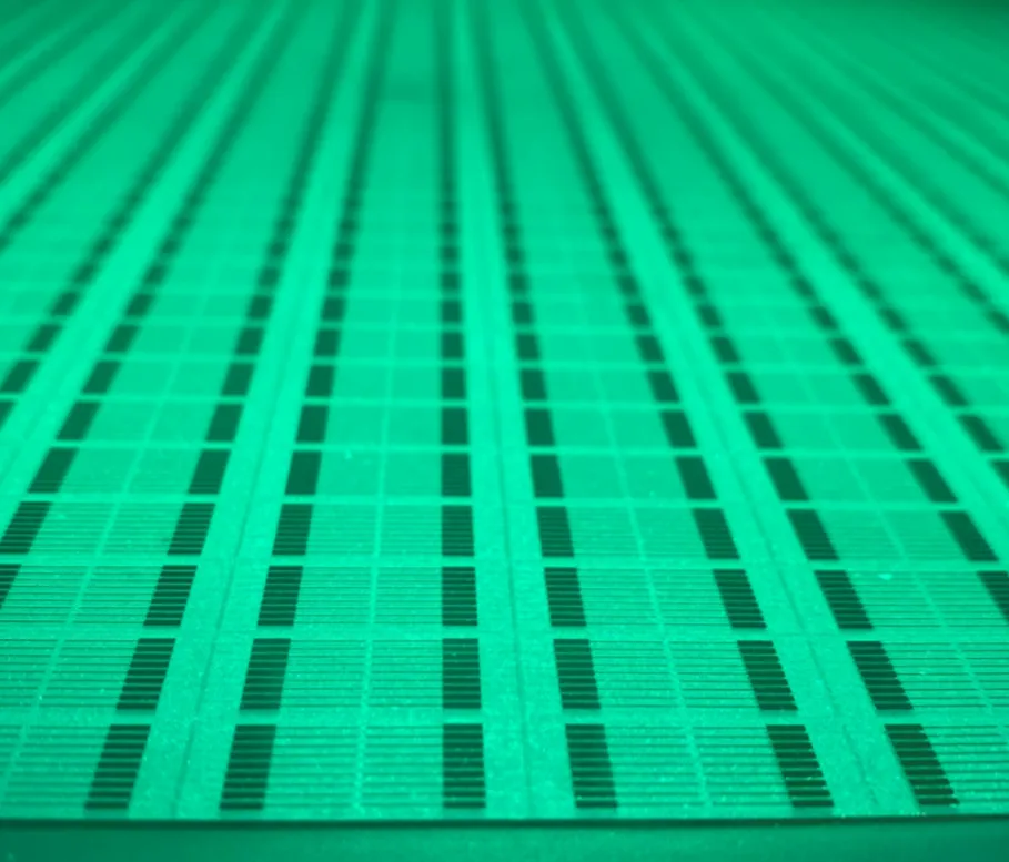
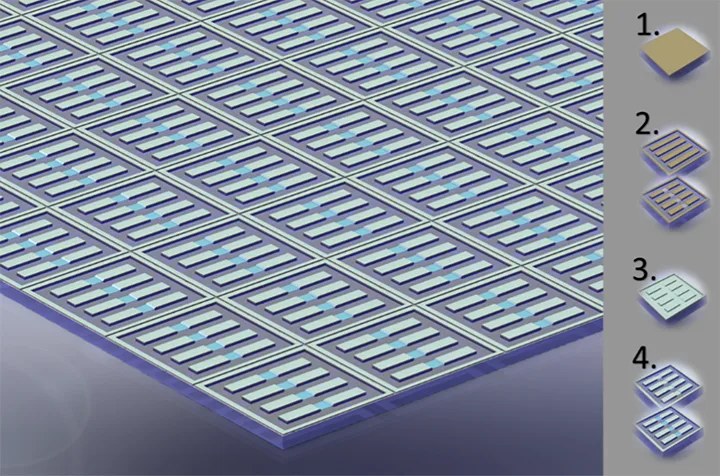
These benefits have been proven by taking a prototype chip-fabrication process which used shadow masks to convert the smooth-blanket sputter coating into a patterned circuit and transitioning it to laser processing. The shadow-mask technique provided a few chips per day, while the laser process provided a dozen chips per minute, including two sputter-deposition steps and two laser-processing steps. Another benefit of laser processing over shadow masks is the consistent edge quality of the features provided by the laser. For this example, further capacity scale-up is possible through the use of production R2R equipment rather than the lab-scale techniques used here.
Without the need to make an upfront geometric commitment, even after full scale-up, design changes may be made to optimize and fine-tune production (see Figure 2). Optimization may include reduction of materials through tuning feature geometry or improving device performance by tuning other process variables. Unlike chemical vapor deposition (CVD) and transfer printing, sputtering together with laser process does not require complex process systems relative to the substrate size and desired manufacturing output. This approach affords tremendous flexibility and breadth in the range of devices that can be produced with a single equipment set.
A multitude of variables
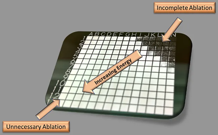
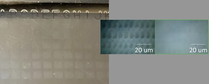
Multiple variables need to be considered for laser processing; a perfect process could be defined as the minimum energy used in the minimum time to achieve 100% usable results. Achieving the perfect process variables means running a large number of tests, incrementally changing variables to generate a grid of different process conditions, and combinations for a range of process conditions can be achieved in a single run with a single laser program. The ratio of energy deposited into the material during patterning by ablation can determine the relationship between laser parameters and minimizes the need for large tests with multiple device evaluations (see Figure 3).
The next phase would be to increase scan speeds and efficiency for processing these variables. Tuning variables could include heating of the substrate, which can cause shrinkage and impact how ejecta interact with the laser beam, thus introducing inconsistency of the ablation. Reflectivity of the patterned materials and morphology of the substrate surface also can impact the results (see Figure 4).
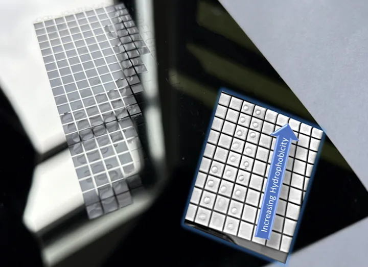
Deposition of the conductive material onto the substrate was done with this firm’s R2R thin-film, vacuum-deposition Lab coater that is available for product and process development. The conductive coating then is laser-patterned to match the desired level of hydrophobicity through morphology between distinct pattern structures, allowing control of the application of selective layers responsible for molecule detection (see Figure 5). Subsequently, specific areas are conditioned to allow for a narrow, continuous 2D-semiconducting material; this is accomplished by depositing the semiconductor material on the entire patterned substrate and then patterning of isolating regions to crystallize them for interfacing with subsequent layers. Once the substrate, layer stacks and laser variables are optimized, the next phase is to scale these devices to large-area R2R processing.
Laser crystallization addresses many concerns
Laser crystallization offers rapid and energy-efficient material processing compared to thermal batch processing. Glass, which often is used as a substrate in 2D electronic devices, can be sensitive to thermal stress and may break or crack if not handled carefully. Polymer-based substrates present even more challenges to batch crystallization due to their poor response to heating and temperature limitations. With laser crystallization, we can selectively target specific areas, minimizing the risk of heat-damage to a substrate. Laser crystallization provides higher efficiency because of this targeted approach which leads to more efficient use of energy, reducing overall production costs as it does away with large inefficient furnaces and full-material heating. Crystallization of thin-film semiconductors using a large-area laser is another innovation that saves a manufacturing step and reduces material handling.
Laser crystallization promises to offer better control over the crystal structure, grain size and orientation of the semiconductor layer, which can result in improved properties and device performance. This level of control is typically more challenging to achieve with thermal crystallization methods.
By adopting R2R manufacturing for flexible-microelectronics devices, we can streamline the production process and significantly reduce labor costs and material handling. Our standard one-button mode of operation simplifies the manufacturing process, lowers the risk of human error, and minimizes the need for manual labor. Roll-to-roll manufacturing introduces even more scalability, allowing for rapid expansion of production capacity as demand increases. For example, a laser head could be added to an existing patterning zone effectively doubling production speed on the same equipment. This scalability ensures that the laser-patterning process can meet the growing needs of the 2D-electronics industry while maintaining consistent quality and performance.
Case studies in flexible 2D-microelectronics device manufacturing
Several research and industry initiatives have successfully employed laser patterning of sputtered coatings for the high-volume production of 2D-electronic devices.
- TMD-based photodetectors: Transition metal dichalcogenides, such as molybdenum disulfide (MoS2), are promising materials for photodetector applications. Laser patterning has been instrumental in creating precise patterns on sputtered MoS2 films, allowing for the fabrication of photodetectors with enhanced light-absorbing capabilities. The resulting devices exhibit high photoresponsivity and can find applications in imaging and optical communication systems.
- Flexible wearable sensors: The flexibility of 2D materials makes them ideal for wearable-sensor applications. Laser patterning has been employed to create flexible and stretchable sensors by selectively patterning sputtered coatings on flexible substrates. This approach has led to the development of wearable sensors that conform to the skin, enabling comfortable and unobtrusive monitoring of physiological parameters.
Challenges and future directions
While laser patterning of sputtered coatings presents numerous advantages, some challenges persist, and ongoing research aims to address them.
- Scalability optimization: Although laser patterning is inherently scalable, optimizing the process for large-scale manufacturing remains a focus of ongoing research. Enhancing the throughput and efficiency of laser-patterning systems will be crucial for meeting the growing demand for flexible 2D-microelectronics.
- Material compatibility: Different 2D materials may require specific laser parameters to achieve optimal results during patterning. Researchers are working to establish guidelines for laser patterning of various 2D materials, taking into account factors such as material composition, thickness and sensitivity to laser energy.
- Cost considerations: While laser patterning offers high precision and efficiency, considerations related to equipment costs and maintenance are essential. Researchers and industry partners are working to develop cost-effective, laser-patterning solutions that balance performance with economic feasibility.
Conclusion
The marriage of laser patterning and sputtered coatings has unlocked new possibilities in the high-volume production of flexible 2D-microelectronics. This innovative approach addresses the demand for devices with enhanced performance, precision, and scalability. A roll-to-roll (R2R) approach offers several significant advantages in terms of efficiency, cost and adaptability. As research in this field continues to advance, the integration of laser patterning into manufacturing processes is poised to play a pivotal role in bringing 2D-device technology to the forefront of diverse industries. The collaborative efforts of researchers, engineers, and industry partners will undoubtedly drive further breakthroughs, leading to the widespread adoption of flexible 2D-microelectronics in applications ranging from healthcare to environmental monitoring and beyond.

Michael Simmons, P. Eng., president & CEO of Intellivation LLC (Loveland, CO) holds a Bachelor of Science in Mechanical Engineering from the University of Idaho. He founded vacuum-coating equipment manufacturer Intellivation in 2009, which has since become a leader in providing R2R vacuum-coating systems and process support. Mike’s extensive background in plasma processing and equipment continues to be enhanced by the installation of a R2R Lab system at Intellivation, which has enabled the company to become a vacuum-process knowledge leader in a wide range of sputtering technologies, deposition control and web handling as well as other PVD techniques. He is a board member of the Society of Vacuum Coaters (SVC), an SVC Instructor for Web Coating, past-chair of the AIMCAL Vacuum Web Coating Committee, an active member of AVS and continuously supports the vacuum community through multiple initiatives. Mike has published multiple technical papers and presented at global conferences. He can be reached at 970-692-2335, email: msimmons@intellivation.com, www.intellivation.com.

