
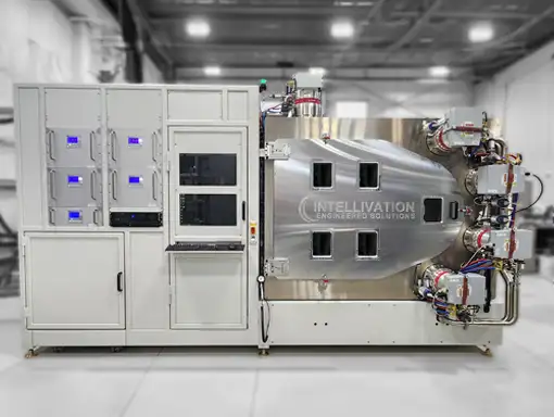
By Mike Simmons, Mark George and Liz Josephson, Intellivation LLC
Producing multilayer dielectric coatings via reactive magnetron sputtering on a large-area web is efficient but challenging due to the need for precise reactive gas distribution and concentration control. Ensuring excellent cross-web and down-web uniformity of the layers is essential for high-tech applications. By using in-situ precision optical methods, cross-web uniformity of reactively deposited dielectric coatings can be measured and adjusted quickly; this is crucial for producing high-performance multilayer coatings.
Characterization of the sputtered layers is done in a roll-to-roll (R2R) sputter vacuum coater by fine-tuning the reactive sputter controller, achieving baseline properties of each single layer. Transitioning to R2R deposition and using in-situ optical measurements ensures satisfactory cross-web uniformity for each single layer, which then sequentially are deposited to form a complex multilayer coating. Validating these processes in-situ accelerates the development of new dielectric materials and multilayer designs.
Introduction
Large-area web coating is a highly efficient method for manufacturing thin film coatings, but there are challenges when it comes to producing sophisticated multilayer dielectric coatings using reactive magnetron sputtering. One of the primary difficulties lies in the control and distribution of reactive working gases, which critically influence the characteristics of the deposited film. Additionally, high-tech applications demand exceptional cross-web uniformity of the film, which requires precise control and monitoring of the reactive sputter process.
The challenge of reactive magnetron sputtering
Reactive magnetron sputtering is a versatile technique for depositing dielectric coatings. Achieving the desired film characteristics involves controlling various parameters. These include magnetic-field strength, target composition, thermal management of the substrate and control of the reactive gases. These factors significantly affect the stoichiometry, optical properties and uniformity of the deposited layers. High-performance applications, such as multilayer optical coatings, require precise control to meet stringent specifications.
The control of reactive gas in the system is one of the key drivers to maintaining quality in these advanced coatings. Flow control is critical because any fluctuation can alter the composition and properties of the dielectric layers, leading to nonuniformities in performance of the end product. The reactive gases, such as oxygen or nitrogen, react with the target material (often a metal) to form the desired stoichiometry and optical properties. Non-uniform distribution can lead to drift in stoichiometry, creating unwanted increases in absorption and thickness variation.
For this work, a 12-layer, alternating high-low index stack was designed and subsequently coated on 2-mil PET film. The principles of developing this multilayer, multipass edge filter can be used for any complex sputter-coating process. Characterizing materials to create processes that are easily transferable to high-volume production in R2R vacuum systems is essential for rapid development and transition to manufacturing. Understanding the process parameters also greatly influences the number of passes needed to manage temperatures of sensitive substrates used in R2R products.
Ensuring cross-web uniformity using in-situ optical monitoring
Variations in film thickness and composition across the web can lead to performance inconsistencies, which are unacceptable in high-tech applications. Advanced in-situ optical methods, such as in-line spectrometer measurements, are used to ensure cross-web uniformity during the deposition process. These methods enable real-time adjustments, ensuring that the deposited films meet the required standards. In optical coatings, any deviation in thickness or composition can result in undesired interference effects, altering the coating’s reflective and transmissive properties. In electronic applications, non-uniform coatings can lead to variations in capacitance or resistance, impacting the device’s overall performance.
Precision optical techniques, such as variable wavelength spectrophotometry, allow for continuous measurement of the film’s optical properties during deposition. This capability enables rapid tuning of the reactive deposition process, ensuring that each layer meets the desired specifications.
In-situ optical monitoring provides several advantages, including immediate detection of any deviations from the desired film properties and enables real-time quality control, which is particularly important in large-scale production, where even minor defects can result in significant material waste and production downtime. In-situ monitoring also supports the development of more complex multilayer structures by ensuring that each layer meets stringent quality criteria before the next layer is deposited. The ability to measure reflection in-situ and in vacuum in the UV, Visible and Mid IR range contributes to the development and process control of a much wider range of functional materials.
Characterization of single layers
The first step in achieving high-quality multilayer coatings involves characterization of the single layers in a R2R vacuum sputter coater. The reactive sputter controller is fine-tuned to deliver baseline properties of stoichiometric single-layer films at high deposition rates without absorption at desired wavelengths. By optimizing control parameters, such as target voltage or optical emission of the plasma, a stable and repeatable process can be established, forming the foundation for subsequent multilayer coating development.
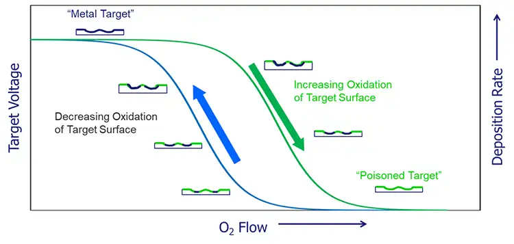
Optimization of the reactive process often is done either through the use of voltage control or the use of a plasma emission monitor (PEM). PEM is used for real-time monitoring of plasma conditions and composition by analyzing the emission spectra of the plasma to determine the presence and concentration of different species. PEM is used for materials with multiple stoichiometries or steep hysteresis curves and unstable voltage, and it helps control to a specific stoichiometry. Voltage control regulates the voltage supplied to the plasma from the power source and is used for materials that have simpler hysteresis effects (see Figure 1).
The hysteresis in Figure 1 is a graphical representation that shows the relationship between discharge voltage and the flow rate of the reactive gas on the state of the sputtering target. With little to no reactive gas flow, the targets are in a metallic state and deposited layers in this region generally are optically absorbing. As the gas concentrations increase, the target moves into the reactive state. This transition region allows for higher deposition rates when the process is stabilized with controls systems, such as PEM. If the region goes beyond to a higher reactive concentration, the poisoned state is reached, which can have good optical properties but significantly reduces deposition rates. A hysteresis shows that increasing and decreasing reactive gas flow and the respective phase changes are different vs. changes in the target voltage.
For the 12-layer stack used in this work, TiO2 and SiO2 were chosen as the high and low index materials, respectively. These two materials commonly are used in a variety of optical applications and have well-established physical and optical properties that can be used to ensure the deposition of quality films. The optical characteristics of a film are specified by the refractive index (n) and the extinction coefficient (k). Each layer needs to be characterized individually to determine process parameters that optimize for both n and k. Single-layer characterization is done on known substrates, such as glass slides or silicon wafers, depending on the optical interference of the material. For the multilayer stack, both the TiO2 and SiO2 need to be characterized independently.
A hysteresis curve is run for the SiO2 from metal state to the poisoned state (increasing gas flow and decreasing voltage), and different points on the curve are selected for deposition of thin films to determine if oxygen content and dynamic deposition rate (DDR) meet the requirements for the specified layer properties and coater throughput. For the low-index layer, SiO2, a silicon wafer substrate is used for an index contrast (n~ 1.45 for SiO2 and ~ 3.96 for Si), which provides large optical constructive interference reflectance maximums and destructive interference minimums that permit straightforward analysis for deposition rate (DDR) and index. During the same runs, layers also are deposited on a glass or quartz slide to measure transmittance of the material to ensure acceptable optical absorption (k).
In a similar method, the high-index TiO2 is measured on glass slides since the index contrast is high enough between TiO2 (n~ 2.4) and glass (n~1.45) to directly measure transmittance and reflection to analyze the thin film to obtain the DDR and optical properties.
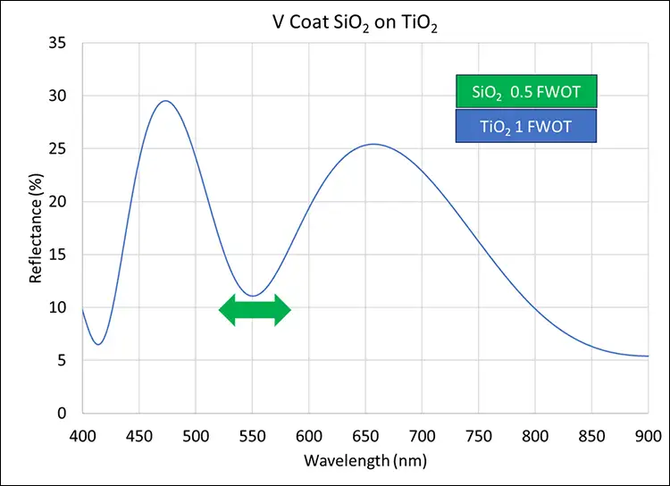
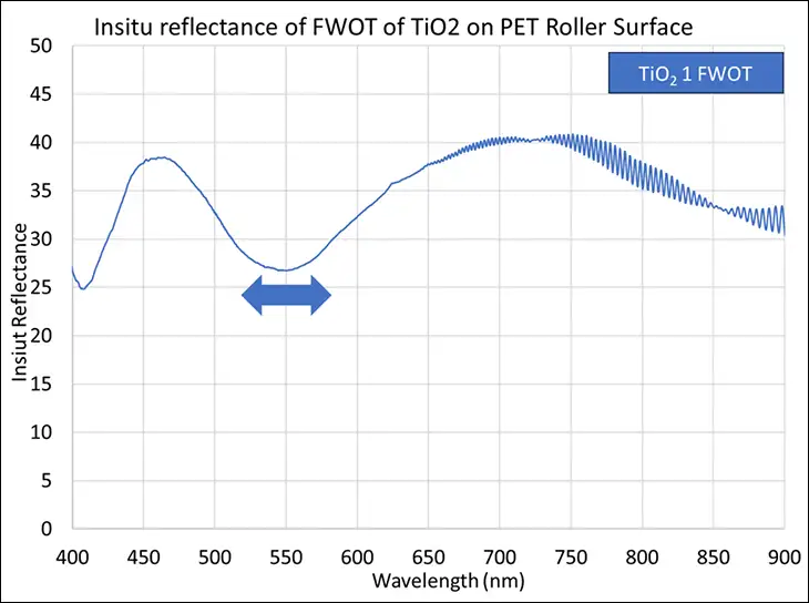
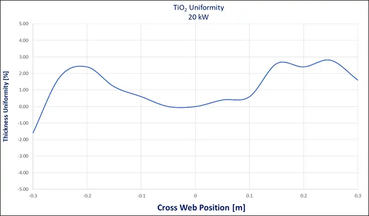
For optimizing cross-web uniformity, a single layer of TiO2 then is deposited on a roll of PET film, since the index contrast between TiO2 and PET (n~1.6) is high enough contrast to provide a large difference in transmittance and reflection, making it easy to measure the uniformity. A FWOT (full wave optical thickness) of TiO2 is deposited that provides a minimum in reflectance at 550 nm (approximately 230 nm physical thickness). The thickness uniformity of the TiO2 is directly proportional to the location of the wavelength minimum (i.e. shorter wavelength is a thinner film). Adjustments are made to the process until the deviation of the wavelength minimum across the web position meets the product specifications. Examples of the reflectance of a single layer of TiO2 is shown in Figure 2 and resulting cross-web uniformity in Figure 3.
To achieve cross-web uniformity of SiO2, a layer is deposited directly on a uniformly TiO2-coated roll using the process conditions established by the previously optimized method. Because the TiO2 uniformity and thickness are known, it is used as reference for the SiO2 “V” coat. A single layer of a ½-wave optical thickness of SiO2 is deposited on the TiO2. Similar to the single layer of TiO2 at the 550-nm minima, the wavelength minimum is directly proportional to SiO2 thickness at half-wave optical thickness (~190 nm), as shown in Figure 4. SiO2 process conditions are adjusted to achieve cross-web uniformity to meet the product specifications.
Transition to R2R mode
The R2R process allows for the continuous deposition of thin films onto flexible substrates, a key advantage for large-scale manufacturing. In the R2R mode, in-situ optical measurements ensure satisfactory cross-web uniformity of each single-layer thin film. These well-characterized individual layers then are sequentially deposited to create the complex multilayer coating.
R2R mode provides significant benefits for high-volume production. The continuous nature of the process enhances throughput and reduces production costs. Additionally, the flexibility of the substrate allows for the production of coatings on a variety of materials, including polymers, ceramics, flexible glass, metals and textiles. This versatility is essential for meeting the diverse needs of different industries, from electronics to healthcare.
Validating the multilayer coating
After the individual layers are deposited, they can be measured in-situ using advanced optical methods, such as ellipsometry and spectrophotometry, to validate that the target spectral designs have been achieved. The ability to quickly verify the coating’s properties accelerates the development process, allowing for rapid iteration and optimization of new dielectric materials and multilayer designs.
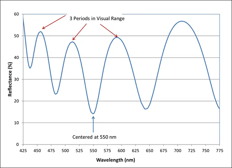
An example of using this method to hit complex coating designs on the first attempt is the design of a multilayer dielectric coating used for edge filters, anti-reflective coatings and mirrors. An alternating high and low refractive-indices stack with three repetitions (or periods) of symmetric stacks is designed and measured; the locations of the reflectance peaks, valleys and amplitudes in the stack’s transmission or reflection spectrum are highly sensitive to thickness and the index of the individual layers (see Figure 5). The slightest variation in layer thickness can shift the interference pattern and change the wavelength position of the peaks (constructive interference) or valleys (destructive interference). Changes in the refractive index affects the optical path length of the light within the coating, altering the interference pattern and optical performance. The system can achieve a resolution of < 0.1% for both thickness and index, allowing for precise control over the optical properties.
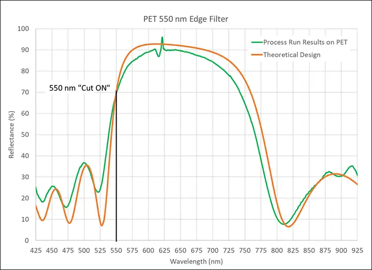
An edge filter is used to sharply separate transmitted and reflected wavelengths; the target is to have a theoretical match of the “Cut On” value required. The “Cut On” value refers to the specific wavelength at which the filter transitions from transmitting to reflecting (or vice versa), typically at 50% reflectance and transmittance. PET commonly is used for R2R edge filters, but the inherent optical properties can affect the performance of a filter and make it challenging to match the exact “Cut On” values (see Figure 6). An edge filter has a substantial bandpass on one side of the limits of the band, creating a precise boundary between the wavelengths that are transmitted and those that are reflected; precision of these coatings is critical for performance.
Applications and benefits
The integration of advanced features in R2R PVD (physical vapor deposition) technology offers numerous benefits for various applications. The ability to produce high-quality, multilayer dielectric coatings with excellent cross-web uniformity and precise control over film properties is essential for applications in medical devices, sensors, microelectronics and more. The scalable production capabilities of R2R vacuum technology enable manufacturers to meet high-volume demands while maintaining the stringent quality standards required for high-tech products.
In the medical field, for instance, precision coatings are crucial for developing advanced diagnostic and therapeutic devices. Multilayer dielectric coatings can be used to enhance the performance of sensors, imaging systems and implantable devices. The ability to produce these coatings with high uniformity and precision ensures their reliability and effectiveness in clinical settings. In the sensor industry, multilayer coatings can improve the sensitivity and accuracy of various types of sensors, including optical, thermal and pressure sensors.
For the microelectronics industry, producing high-quality dielectric coatings is critical for developing advanced electronic components, such as capacitors, resistors and transistors. These components form the building blocks of modern electronic devices and their performance directly impacts the functionality and reliability of the final product. Optical filters can be designed to serve a wide range of applications by tailoring layers for different durability requirements, including environmental impact. Sputter-coated thin films offer precise layer control, stability and durability to meet specific optical properties that allow increased range and low noise without interference from environmental changes.
Future directions and innovations
As the demand for high-performance coatings continues to grow, ongoing research and development in R2R vacuum technology are driving new innovations. One promising area of development is the integration of advanced materials, such as nanomaterials and novel dielectrics, into the R2R coating process. These materials offer unique properties that can further enhance the performance and functionality of multilayer coatings.
Another area of innovation is the development of more sophisticated in-situ monitoring and control systems that increase the optical band spanning from the UV to the Far Infrared. Advances in optical sensing technologies, such as hyperspectral imaging and machine-learning algorithms, are enabling more precise and automated control of these deposition processes. These technologies can further enhance the accuracy and efficiency of R2R vacuum systems, reducing production costs and improving product quality.
Additionally, there is a growing interest in sustainable manufacturing practices within the industry. Researchers are exploring ways to minimize the environmental impact of the R2R vacuum process, including the reduction of energy consumption and the development of eco-friendly materials. Sustainable practices not only benefit the environment but also enhance the long-term viability of the technology by reducing operational costs and meeting regulatory requirements.
Conclusion
Large-area web coating using reactive magnetron sputtering presents unique challenges, particularly in achieving the desired film characteristics and cross-web uniformity for multilayer dielectric coatings. By leveraging advanced in-situ optical monitoring and precision control of the deposition process, these challenges can be effectively addressed. The ability to directly transition from individual layer characterization to multilayer R2R deposition enables rapid development and scalable production of sophisticated multilayer coatings, driving innovation and enhancing performance across a wide range of applications.

Michael Simmons is president and CEO of Intellivation LLC, a vacuum coating equipment manufacturer he founded in 2009. Mike is responsible for designing, manufacturing and installing a wide variety of equipment over the past 15 years, from production vacuum deposition R2R tools to R&D systems and automation machinery. Roll-to-Roll vacuum deposition is the primary focus for Mike and his team, as exemplified by Intellivation’s innovative R2R series product line. Mike’s extensive background in plasma processing and equipment continues to be enhanced by the installation of an R2R Lab system at Intellivation. His commitment to the industry involves being a Board of Director of Society of Vacuum Coaters (SVC), an SVC Instructor for Web Coating, Chair of ARC’s Vacuum Web Coating Committee, RMCAVS Chair, an active member of AVS and continuous support of the vacuum community through multiple initiatives and sponsorships. Mike earned his mechanical engineering degree (BSME) from the University of Idaho. He can be reached at: 970-692-2335; email: [email protected]; www.intellivation.com.