
By Robert Malay, Ph.D., product development engineer, VDI
Introduction
In 1999, British technology entrepreneur Kevin Ashton first coined the term, “The Internet of Things,” or IoT. Ashton described the IoT as “the internet being connected to the physical world through the presence of ubiquitous sensors.” These sensors could detect and interpret stimuli in their environment and send signals back to various devices in reaction to what happened. Fast forward 20 years, and it is easy to see how this has taken shape in modern life. Cellphones communicate with FitBits to keep track of your health throughout the day. Refrigerators can send messages to your email when certain groceries are low or when the water filter is about to expire. Alexa lets you change your thermostat, check your security cameras, call your spouse and play the music on your PC – all without having to get up from the couch. The IoT already has become a reality in everyday life.
Because the technology that allows this easy intercommunication now is well established, the next step in integrating communication with various objects is the development of sensing technology that can be applied to different media. Sensors that are flexible and conformable have long been desired for their ability to be applied retroactively to different materials and objects. With flexible and flexible hybrid electronics (FHE), the thin and bendable nature of devices makes them suitable for irregular geometries. With an increasing amount of these types of electronics in the market, roll-to-roll (R2R) web processing now is increasingly important in making these devices in a cost-effective, repeatable manner, while also allowing for some functionality that may not be feasible with rigid substrates.
More and more techniques have seen integration into R2R systems, which allow for full fabrication of devices in roll format. Physical and chemical vapor deposition (CVD) techniques have seen widespread use for many years. Wet and dry etching have been demonstrated in R2R format for various materials such as metals, oxides, nitrides and other common electronics materials. And with the development of patterning techniques that allow for fine alignment between layers, such as nano-imprint lithography and projection lithography, the ability to fabricate devices completely R2R allows for a variety of avenues of product manufacturing.
Multi-functional medical sensors a key application
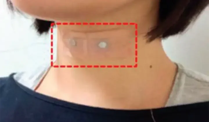
![FIGURE 1. Sensor located at tracheal region of neck [1]](https://convertingquarterly.com/wp-content/uploads/2025/02/cq420pfe-malay-Figs-1.webp)
The designs and layouts of flexible electronics often can be complex, with multiple systems required for the desired functionality. One of the highest demand areas for flexible sensors and devices is that of medical sensors that can be worn and autonomously communicate with other devices. Huynh and Haick [1] have shown multiple avenues to integrate autonomous power systems into flexible health sensors. Figure 1, recreated from their paper, shows application of a flexible sensor to a patient’s throat. The sensor has the ability to monitor multiple outputs, such as breathing, coughing, drinking and eating. It can be used to diagnose and monitor the patient’s biological functions over time and can be used to trigger an alarm if abnormal behavior is observed.
These sensors already are equipped with multiple systems. Sensing interfaces serve to interpret inputs from the outside environment, whether from the patient or otherwise, and generate a signal. Various transducer arrays can convert that signal to any form needed. Transistor arrays can perform any secondary-logic function that may be necessary, either for user input, data storage or logic functions. Antennae are present for communication, usually via a Bluetooth connection or similar protocol. Autonomous power systems also can be included that would allow for self-powered, self-sensing and self-healing properties throughout the device.
Spiders, earthquakes and robots
![FIGURE 2. General device design and potential applications for spider-inspired, flexible vibration sensor [2]](https://convertingquarterly.com/wp-content/uploads/2025/02/cq420pfe-malay-Figs-2.webp)
Other areas of interest for flexible electronics include sensors for vibration and mechanical analysis. This is an interesting area of application, as it relates not only to the healthcare sensors described above (heartbeat, respiration, body-movement, etc., are all mechano-vibrational phenomena that can be measured effectively) but also to industrial and infrastructural applications.
Vibrational analysis can be critical to investigating a variety of criteria, from process-engineering challenges in factory equipment to structural and safety analysis for large structures. Using flexible sensors, vibrations and mechanical stress can be investigated and analyzed by simply applying these sensors to the area of interest. Added functionality of communication between sensors and from sensor to device (often via Bluetooth) can make real-time vibrational analysis possible and relatively simple. Some proposed applications for these sensors include earthquake warning and analysis to determine if the stability of buildings is cause for concern during these events.
This type of instant application of devices to existing infrastructures is a great advantage for flexible electronics. Adhesives coated to a device’s backside allow for easy application to different surfaces. If these devices are capable of autonomously sensing data (i.e., an adhesive doesn’t interfere with a sensor system) and have the ability to wireless communicate, it becomes straightforward to apply these to existing structures, such as bridges and buildings. Liu et al provide an example of a mechano-vibrational sensor that can used across multiple industries. These sensors then can be used to remotely monitor structural integrity and alert in real-time when any cause for concern arises. Figure 2 illustrates the different applications. In much the same way a health sensor will monitor a patient continuously, these sensors provide the potential for continuous monitoring of our infrastructure, like the aforementioned bridges, but also can assist in analysis of traffic flow, supply chains, engineered processes and more.
Fabrication of each of the necessary systems described above has been demonstrated in fully R2R-converting systems. In much the same way as the semiconductor industry, deposited thin films are patterned and etched into a variety of devices. Reported single-layer devices have seen success in being competitive with existing rigid devices. Most notable of these are touchscreen modules and barrier films, which require minimal patterning and etching steps to realize functionality.
A fine line for alignment
The greatest obstacle to widespread use of R2R processing for flexible-electronics fabrication is the requirement of fine alignment for multilayer devices. Layer registration for devices on rigid substrates has been better than +/-1 micron for years. However, registration on flexible substrates has proven a challenge due to the changing dimensions of polymer webs. Thermal and mechanical stress, often arising from processing and simple web conveying, can cause elongation and distortion. This change in dimension often easily is greater than the total feature size that has been patterned and leads to critical device failure and defective rolls.
Successful layer-to-layer pattern registration has been realized using a number of methods, most of which compensate for the above challenges of thermal and mechanical deformation. Some equipment, such as step-and-repeat printers, are equipped with feature-offset magnification, which allows for automatic readjustment of feature position in both the transverse (TD) and machine directions (MD) of the web. This enables versatile fabrication that can use a wide variety of processing inputs and device designs without compromising the R2R functionality. Devices patterned in this method include thin-film, metal-oxide semiconductor field-effect transistors (MOSFET), antenna arrays and interposer substrates for 3D-IC (integrated circuit) applications.
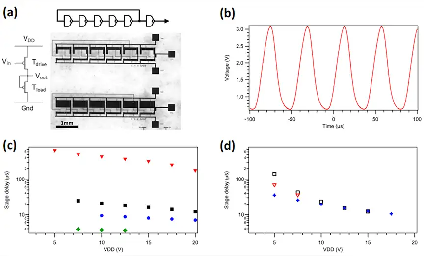
Other methods to overcome these difficulties also have been demonstrated. Gold et al report using self-alignment strategies to fabricate complex devices on organic substrates using R2R-capable techniques [3]. Self-aligned organic thin-film transistors (OTFTs) and five-stage ring-oscillators have been demonstrated using nano-imprint lithography as a patterning method. It has been reported that ring oscillators fabricated by this method demonstrate average stage-delay below 4 µs at 7.5 V, which is competitive with similar devices being reported with conventional fabrication methods. Figure 3 shows the performance of these ring oscillators after fabrication [3].
More than just polymer films and coating
![FIGURE 4. Schematic shows steps for assembly of stretchable AM-LED display by triple overlay-aligned roll transfer [4].](https://convertingquarterly.com/wp-content/uploads/2025/02/cq420pfe-malay-Figs-4.webp)
Overlay-aligned roll-transfer printing has been shown to be effective at device design and fabrication for flexible components. Layers that often are difficult to fabricate R2R can be developed and deposited onto rigid substrates that then can be transferred to roll material. This is useful for layers that may require high-temperature annealing or other sensitive processes. Choi et al demonstrate this technique by fabricating an inorganic LED via a combination of roll processing and transfer printing [4]. Figure 4 shows a diagram of the techniques used. This combination allows for as many processes that are realistic for rolled material to be performed, while keeping the advantages of rigid processing. This process may not be as cost-efficient as a fully R2R process, but it alleviates much of the batch-cost associated with panel processing of flexible electronics.
In addition, new techniques that enable devices to be patterned R2R, along with the advent of exciting new materials being used in place of traditional polymer films, allow many different types of devices. Included in these materials are flexible glass and ceramics, which are capable of being wound through roll systems as if they were polymer films. Electronic devices such as interposers, TFTs, antennae and anti-reflective coatings already have been demonstrated, with continued work on the reliability of processing these once fragile materials [5]. The integration of these materials to rolled systems allows for system design that may yield better-performing devices with improved optical properties and electrical performance.
Conclusion
As more technologies emerge for R2R development of traditionally rigid electronics, the push toward the lower costs afforded by R2R processing becomes a realistic option. There now exist avenues to overcome some of the biggest challenges in manufacturing flexible electronics via R2R. Multiple types of devices have been demonstrated on flexible substrates, and autonomous capability shows promise for long-lifetime devices. With processes demonstrable on a web, R2R processing will prove critical in providing a cost-effective path toward an interconnected (IoT) infrastructure.
References
- Huynh, T., Haick, H. (2018). Autonomous Flexible Sensors for Health Monitoring. Advanced Materials, 30(50), 1802337. doi:10.1002/adma.201802337
- Liu, Y., Liu, Q., Li, Y., Huang, P., Yao, J., Hu, N., & Fu, S. (2020). Spider-Inspired Ultrasensitive Flexible Vibration Sensor for Multifunctional Sensing. Applied Materials and Interfaces, 12, 30871-30881. doi:10.1021/acsami.0c08884.s001
- Gold, H., Haase, A., Fian, A., Prietl, C., Striedinger, B., Zanella, F., Stadlober, B. (2015). Self-aligned flexible organic thin-film transistors with gates patterned by nano-imprint lithography. Organic Electronics, 22, 140-146. doi:10.1016/j.orgel.2015.03.047
- Choi, M., Jang, B., Lee, W., Lee, S., Kim, T. W., Lee, H., Ahn, J. (2017). Stretchable Active Matrix Inorganic Light-Emitting Diode Display Enabled by Overlay-Aligned Roll-Transfer Printing. Advanced Functional Materials, 27(11), 1606005. doi:10.1002/adfm.201606005
- Malay, R., Nandur, A., Hewlett, J., Vaddi, R., White, B E., Poliks, M.D., Pollard, S.C. (2015). “Active and passive integration on flexible glass substrates: Subtractive single micron metal interposers and high performance IGZO thin film transistors.” 2015 IEEE 65th Electronic Components and Technology Conference (ECTC). doi:10.1109/ectc.2015.7159667
Robert Malay, Ph.D., product development engineer at Vacuum Depositing (VDI) in Louisville, KY, holds a BS in Chemistry, as well as an MS and Ph.D. in Industrial and Systems Engineering from Binghamton University. He has been with VDI since 2018, serving as the Product Development Manager and later Technical Manager. Malay oversees all product development and process engineering. He brings over five years of experience in both vacuum coating and the electronics industry, including fabrication processes such as sputter and vapor deposition, analytical techniques, research methodology and Lean/Six Sigma experience. Malay serves as the co-chair for the Vacuum Web Coating Committee at AIMCAL. He can be reached at 502-969-4227, email: rmalay@vdi-llc.com, www.vdi-llc.com.