
By Matthew Dyson, Ph.D., technology analyst, IDTechEx
Abstract
Printed and flexible electronics represent an exciting alternative to conventional manufacturing methodologies, with a wide range of end-use applications. These span from the technically sophisticated, such as OLED displays and image sensors, to comparatively low-value but high-volume applications, such as smart packaging. Although at present OLED displays dominate the market by value, there are technical innovations occurring across the printed & flexible electronics (PFE) applications space that enable new capabilities and more cost-effective manufacturing methodologies. Here, both market forecasts and the development of new technologies to enable roll-to-roll (R2R) manufacturing across the application space will be discussed.
Introduction
At first glance, it appears that a high-end OLED TV and a simple RFID tag have little in common. However, both fall under the umbrella of printed and flexible electronics, with similarities in materials and viable production methodologies. The “printed” aspect requires at least part of the functional materials in the circuit to be dispensed from solution, while the “flexible” aspect requires at least part of the circuit to be mounted onto a flexible, perhaps even stretchable, substrate. Although some technologies can be printed and not flexible (i.e., printing conductive ink onto injection-molded plastic) or flexible and not printed (i.e., flexible circuit boards (PCBs) with conductive interconnects that are etched copper on polyimide), the two terms normally go together. This is because solution processing intrinsically is compatible with thermally fragile, flexible substrates, such as widely used polyethylene terephthalate (PET).
This article sets out where IDTechEx sees the biggest opportunities for printed and flexible electronics (PFE), with a focus on applications amenable to high-volume continuous processing. Current market values are estimated, and market growth over the next decade forecasted. The technical challenges required to realize these applications, and the associated innovation opportunities, also are analyzed.*
Flexible hybrid electronics
An important emerging trend within the printed & flexible electronics space is flexible hybrid electronics (FHE). This approach aims to combine the best attributes of printed electronics – such as flexibility, low weight and customization – with the processing capability of mounted inorganic components, thus meeting market requirements rather than being constrained by a particular set of materials and manufacturing methodologies. FHE is highly relevant to those engaged in converting and continuous manufacturing. This is because it should enable a transition from manufacturing PCBs in a sheet-to-sheet (S2S) fashion to printing conductive interconnects onto flexible substrates, at least for applications where flexibility, low weight and low cost are valued over circuit complexity.
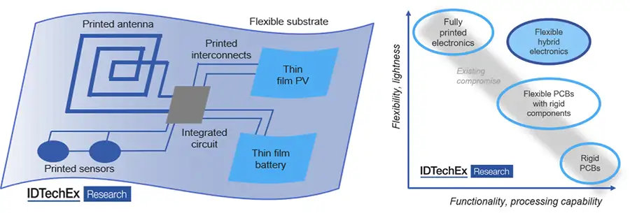
Figure 1 shows a prototype FHE circuit, demonstrating how both printed and placed components can be integrated into the same circuit. The basic principle can be described as “print what you can, place what you can’t.” In this example, the antenna, sensors and interconnects are all likely to be printed, while the organic photovoltaic (OPV) cell and battery will be either printed or placed, and the integrated circuit (IC) will be placed.
You might think that this combination of processing capability and flexibility already has been met by flexible PCBs. However, these generally have rigid islands to solder packaged components onto, require expensive polyimide substrates and have conductive interconnects made from etched copper. In contrast, FHE is likely to use flexible ICs (based on either thinned Silicon or metal oxide), has conductive interconnects printed onto cheaper flexible substrates and uses low-temperature-component attachment methods. As shown in Figure 1, this combination breaks the existing compromise between flexibility/lightness/cost and functionality/processing capability, making FHE a very compelling manufacturing approach.
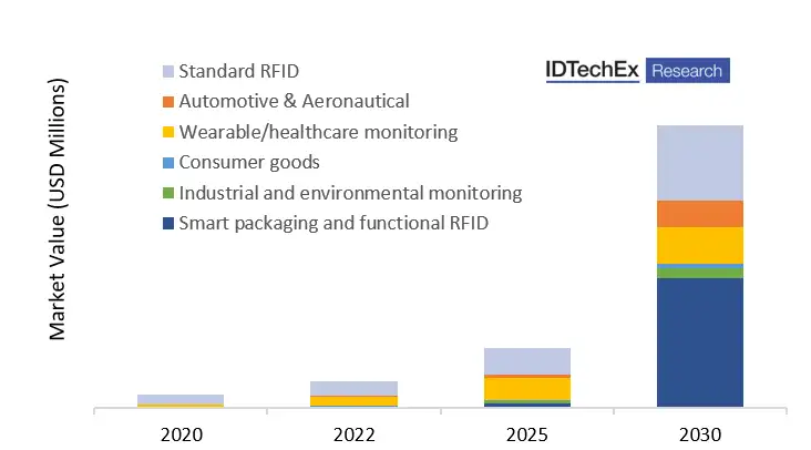
Figure 2 shows our forecast for the adoption of FHE across different sectors. We believe that smart packaging and wearable technology are the most promising applications, with wearable technology likely to show the greatest initial growth.
Smart packaging
The PFE application with the most relevance to the R2R converting community is smart packaging, which is highly likely to adopt the FHE approach outlined above. The main selling points of smart packaging are that it enables manufacturers of consumer goods to both improve the customer experience and acquire detailed, granular data on what products experience during their entire life cycle. Imagine electronics and sensors incorporated within the packaging for food and consumer goods that communicate with the cloud to order replacements or alert you to an approaching expiration date. Alternatively, consider the commercial attractions of incorporating accelerometers, touch sensors or even displays into consumer products, allowing the user to interact with the product and allowing manufacturers to determine how their products are used.
IDTechEx forecasts that, much like RFID tags, smart packaging will take multiple years to move from technical feasibility to widespread adoption. However, we believe that it will see substantial growth toward the end of this decade. One of the main challenges for smart packaging adoption in applications such as food is making it at a sufficiently low cost to add to what often are single-use, disposable items. In addition to the technical challenges – such as incorporating electronics-manufacturing technologies (pick-and-place) into high-volume, continuous packaging lines – there also are commercial difficulties. The most important is that generating value requires an entire ecosystem, such as domestic appliances that interact digitally with consumer goods, thus creating a Catch-22 situation that requires substantial simultaneous investment from companies in different sectors to resolve.
The initial applications for smart packaging are likely to be those that add the most value, and thus don’t necessarily require a fully developed ecosystem. One such example is integrating electronic sensors and wireless-communication capability into pharmaceutical packaging. This could send a notification to the cloud whenever a tablet is removed from the blister pack, enabling monitoring of patient compliance with a prescription. For example, it could enable patients to receive a smartphone notification if a tablet was not removed within a certain timeframe, while adding GPS capability could enable health authorities to track controlled substances.
Wearable electronics
Another highly promising PEF application is wearable technology, especially for healthcare and fitness applications. “Wearables” span a wide range of technologies, from rigid items such as smart watches and hearing aids to genuinely flexible electronics such as skin patches and e-textiles. FHE is highly applicable to the latter as, along with the aforementioned benefits, digital-printing methods (unlike etching) enable customization to suit different end-use requirements.
At present, most e-textiles and skin patches are manufactured using a “rigid island” approach. While the electrodes and conductive interconnects generally are printed onto flexible or even stretchable substrate such as fabric or TPU, the bulk of the electronics remain in a rigid plastic box. This means that conventional electronics-manufacturing processes can be used but make the patch or clothing bulky and uncomfortable. Over time, electronics will become more integrated with the patch itself, using the FHE approach outlined above. This transition will require stretchable conductive inks that are sufficiently durable to withstand washing, along with robust component-attachment methods that can tolerate the different thermal expansion coefficients of rigid components and plastic/textile substrates.
Sensors
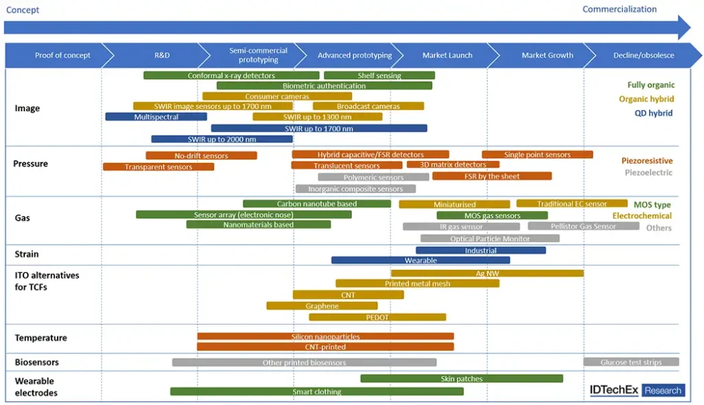
Printed & flexible sensors are essential components of printed electronics. It is an incredibly diverse field, with technologies ranging from hybrid image sensors to transparent conductive films for capacitive touch screens. The schematic in Figure 3 shows our assessment of the commercial readiness levels of each sensor technology.
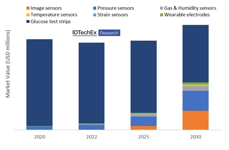
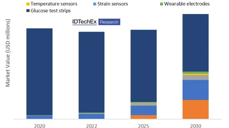
Considering the size and prospects of the printed-sensor market, by far the dominant application is glucose test strips (see Figure 4). With tens of millions of diabetics around the world requiring multiple test strips a day, it is easy to see how this is a multi-billion-dollar application. However, dispensing a drop of blood onto a printed strip of paper is inconvenient and gradually is being replaced by continuous glucose monitoring. Applications for pressure sensors (smart flooring) are likely to grow substantially, as are image sensors (especially hybrid image sensors for short-wavelength infrared (SWIR) imaging).
Printed and flexible batteries
Most of the applications discussed so far require some sort of power source. While this can involve forms of energy harvesting (photovoltaics, thermoelectrics or even harvesting of electromagnetic radiation), generally energy storage also is required. As such, printed batteries have been the subject of extensive interest. Along with the technical challenges that one would associate with all batteries, such as maximizing energy capacity and enabling high charge/discharge rates, the tolerance to bending and ease of manufacture must be considered for printed & flexible batteries.
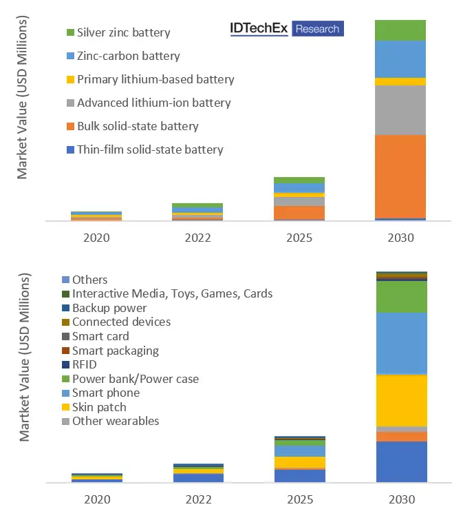
IDTechEx predicts substantial growth in the printed & flexible battery market over the next 10 years, with much of the growth occurring in skin patches and backup energy storage (see Figure 5). Solid-state technologies are likely to dominate because of increased durability and safety relative to alternatives with a liquid electrolyte.
Printed and flexible displays
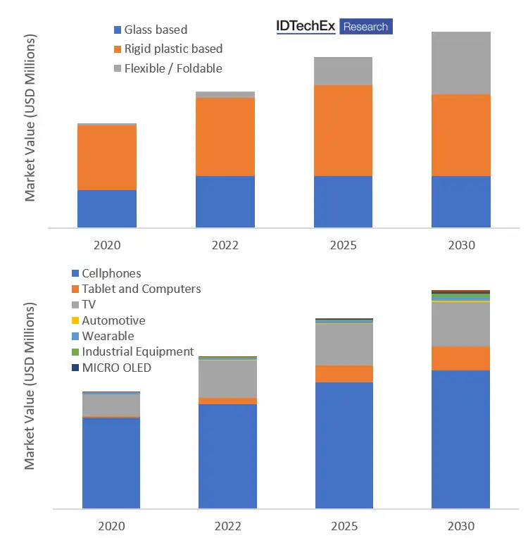
Arguably the most successful commercial PFE application is OLED displays, which can be found in many smartphones, televisions and computer monitors. Although OLEDs widely are included within the scope of PFEs, almost all OLED displays today are based on small semiconducting molecules that are thermally evaporated onto glass substrates. However, OLED materials are compatible with both thermally fragile, flexible substrates and solution processing. As such, over the last year or so, flexible-OLED displays have emerged on the market, and many manufacturers are investigating printing of OLED materials as an alternative manufacturing. Our forecast for OLED displays is shown in Figure 6, indicating that much of the growth will occur in flexible and foldable displays.
Along with OLEDs, other display types also can be made flexible. One area of innovation is in flexible backplanes made with organic thin-film transistors. These currently are in the development stages and are best suited to electrophoretic and LCD displays where the current (and hence charge-mobility) requirements are lower.
Innovation opportunities for R2R manufacturing
While the vision of replacing sheet-to-sheet (S2S) manufacturing of PCBs with R2R production that combines printed conductive interconnects with placed components is compelling (and highly relevant to the converting community), substantial technical challenges remain. Chief among these is the difficulty of securely and rapidly attaching surface-mount components to flexible substrates. The first challenge is that soldering requires high reflow temperatures, and hence thermally robust substrates such as polyimide (PI). This is the approach used for flexible circuit boards at present, with PI providing the characteristic orange color. However, PI is far more expensive than transparent, thermally fragile substrates such as PET or PEN, meaning that existing approaches are not compatible with high-volume applications. As such, much effort is being devoted to low-temperature, component-attachment methods, ranging from ultralow-temperature solder alloys to innovative, anisotropic conductive adhesives.
Another technical challenge is placing the components. At present, components are mounted using pick-and-place, but this is slow and vacuum gripper heads are not especially well suited to handling flexible components such as thinned silicon dies. Achieving precise alignment with flexible (and especially stretchable) substrates also has its technical challenges at high speeds. Alternatives to pick-and-place, notably direct transfer from wafer to substrate using a needle or by vaporizing an adhesive with a laser, are being developed but are yet to be widely adopted.
Conclusion
Perhaps the most significant opportunity, especially for companies in the converting industry, is that there has been an acceptance in the last few years that the most promising PFE applications do not have to rely on printed electronics entirely. Instead, they can combine printed interconnects and components with conventional microprocessors to bring together the best of both technologies. Crucially, this approach – termed flexible hybrid electronics (FHE) – is applicable across a wide range of applications.
In summary, we believe that there are extensive and varied opportunities for printed & flexible electronics. While OLED displays likely will remain the dominant market segment, less-complex and lower-value applications are projected to grow substantially. In addition to the obvious benefits of flexibility, the reduction in weight and compatibility with rapid prototyping enabled by digital, additive manufacturing are a substantial contributor to the overall value proposition.
Matthew Dyson, Ph.D., technology analyst with IDTechEx (Cambridge, UK), holds an M.Res. and a Ph.D. in Physics from Imperial College London, in which he specialized in printed electronics, specifically processing-structure-property relations in organic semiconductors. More recently, Dyson completed two years of post-doctoral research at Eindhoven Technical University/Holst Centre, primarily investigating trap states and their effect on organic photodetectors. At IDTechEx, his recent work has covered flexible hybrid electronics, printed and hybrid sensors, 3D electronics and materials for printed electronics. Dyson has co-authored 13 scientific papers, collaborated with multiple institutions around the world and presented his research at a variety of international conferences. He can be reached at +44-1223-810-281, m.dyson@idtechex.com.
* Detailed, granular forecasts, company profiles, technological readiness assessments and rigorous technical analysis can be found in the relevant IDTechEx reports, available at www.idtechex.com.